

Semiconductor Device and Method for Fabricating the Same
a technology of semiconductor devices and semiconductors, applied in the direction of semiconductor devices, basic electric elements, electrical equipment, etc., can solve the problems of parasitic capacitance, affecting the characteristics of the device, and the operation speed of high-integration devices, so as to increase parasitic capacitance and reduce the operation speed of the device
- Summary
- Abstract
- Description
- Claims
- Application Information
AI Technical Summary
Benefits of technology
Problems solved by technology
Method used
Image

Examples
Embodiment Construction
[0011]Reference will now be made in detail to the embodiments of the present disclosure, examples of which are illustrated in the accompanying drawings.
[0012]In the following description, it will be understood that when a layer (or film) is referred to as being ‘on / over’ another layer or substrate, it can be directly ‘on / over’ the other layer or substrate, or intervening layers can also be present.
[0013]In the drawings, the thicknesses or dimensions of layers and regions are exaggerated for clarity of illustration.
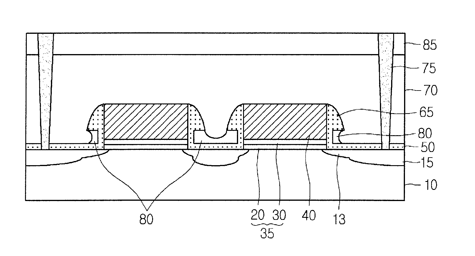
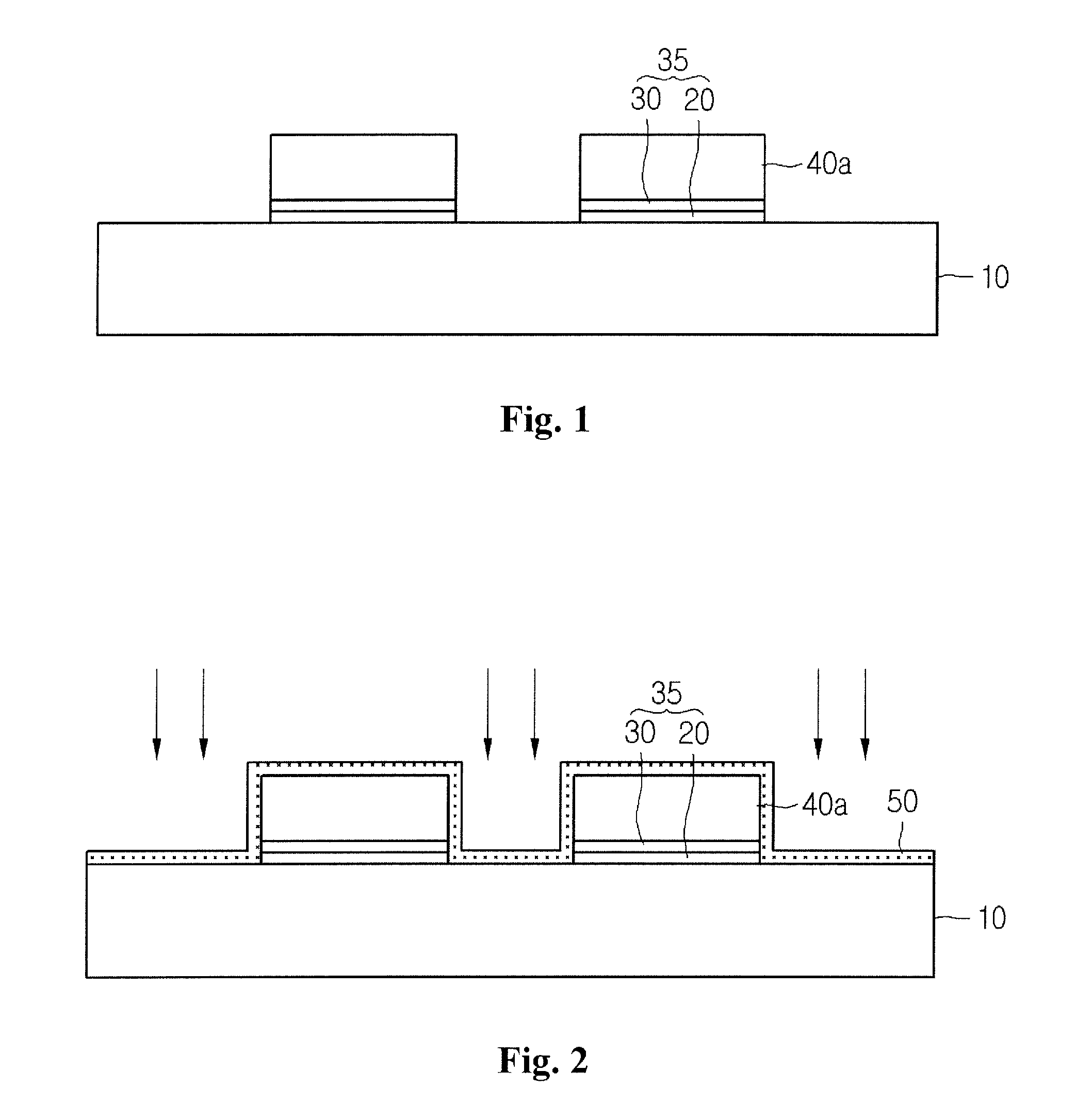
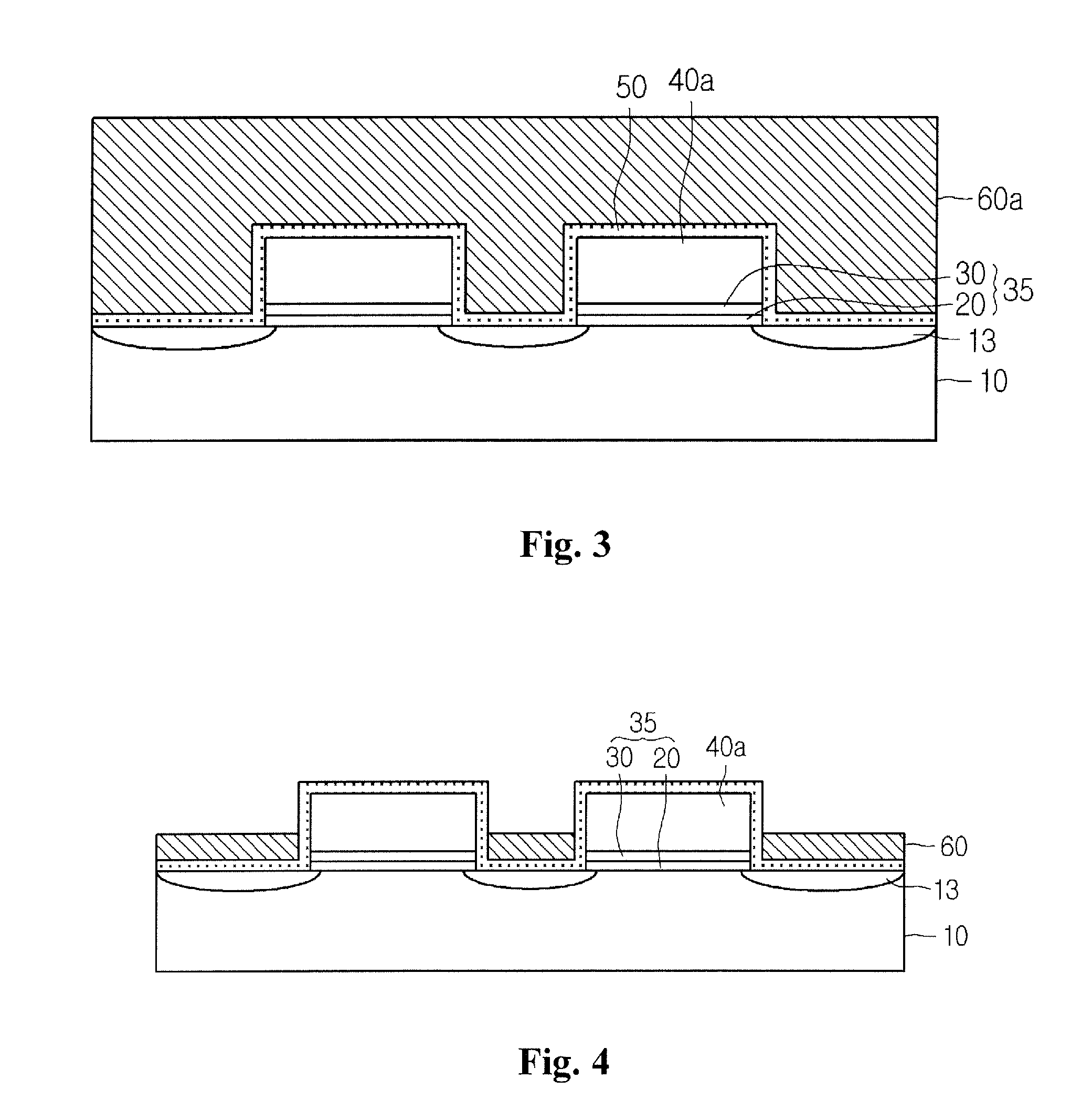
[0014]Referring to FIG. 12, a semiconductor device according to an embodiment includes a gate dielectric 35 and a gate electrode 40 stacked on an active region of a semiconductor substrate 10.
[0015]A lightly doped drain (LDD) region 13 and a source / drain region 15 can be provided in a region of the semiconductor substrate 10 about the gate. Spacers 65 can be formed at sidewalls of the gate dielectric 35 and the gate electrode 40. In an embodiment, the spacers 65 are formed...
PUM
 Abstract
Description
Claims
Application Information