
Method for adjusting a transistor model for increased circuit simulation accuracy

a transistor model and circuit simulation technology, applied in the field of semiconductor device modeling, can solve problems such as the inability of transistor models to provide accurate circuit simulation, and achieve the effect of increasing circuit simulation accuracy

Active Publication Date: 2008-11-20
ADVANCED MICRO DEVICES INC
View PDF2 Cites 8 Cited by
  • Summary
  • Abstract
  • Description
  • Claims
  • Application Information

AI Technical Summary

Benefits of technology

[0004]A method for adjusting a transistor model for increased circuit simulation accuracy, substantially as shown in and / or described in connection with at least one of the figures, and as set forth more completely in the claims.

Problems solved by technology

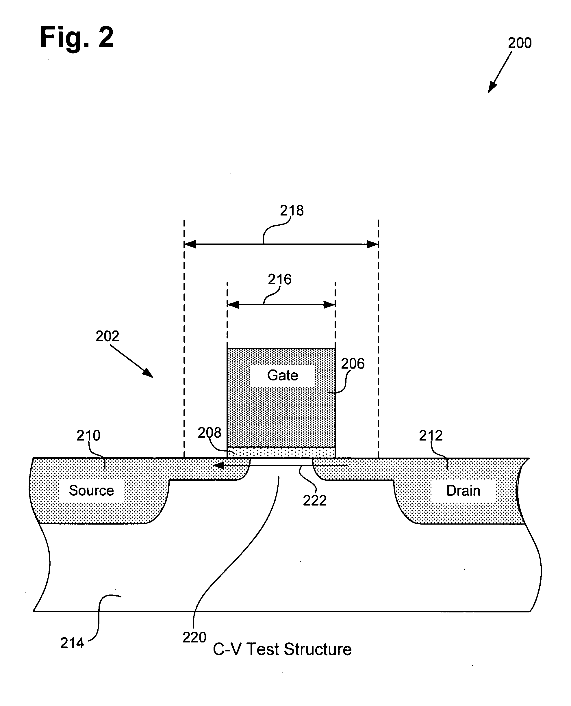
If the transistor model is not adjusted for the difference in gate length between the I-V and C-V test structures, the transistor model may not provide accurate circuit simulation results.

Method used


Image

  • Method for adjusting a transistor model for increased circuit simulation accuracy
  • Method for adjusting a transistor model for increased circuit simulation accuracy
  • Method for adjusting a transistor model for increased circuit simulation accuracy

Examples


Embodiment Construction

[0012]The present invention is directed to a method for adjusting a transistor model for increased circuit simulation accuracy. The following description contains specific information pertaining to the implementation of the present invention. One skilled in the art will recognize that the present invention may be implemented in a manner different from that specifically discussed in the present application. Moreover, some of the specific details of the invention are not discussed in order not to obscure the invention.

[0013]The drawings in the present application and their accompanying detailed description are directed to merely exemplary embodiments of the invention. To maintain brevity, other embodiments of the present invention are not specifically described in the present application and are not specifically illustrated by the present drawings.

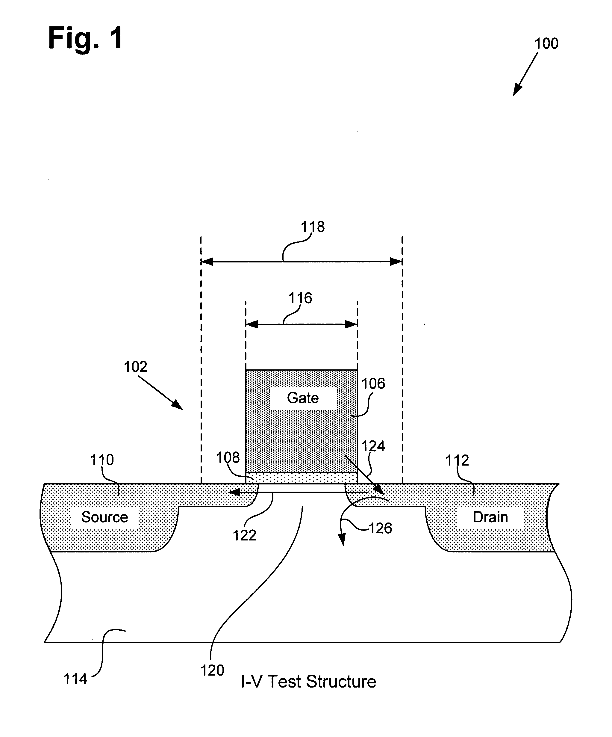
[0014]FIG. 1 shows a cross-sectional view of structure 100, which includes an exemplary I-V (current-voltage) test structure situated on a ...


PUM


Abstract

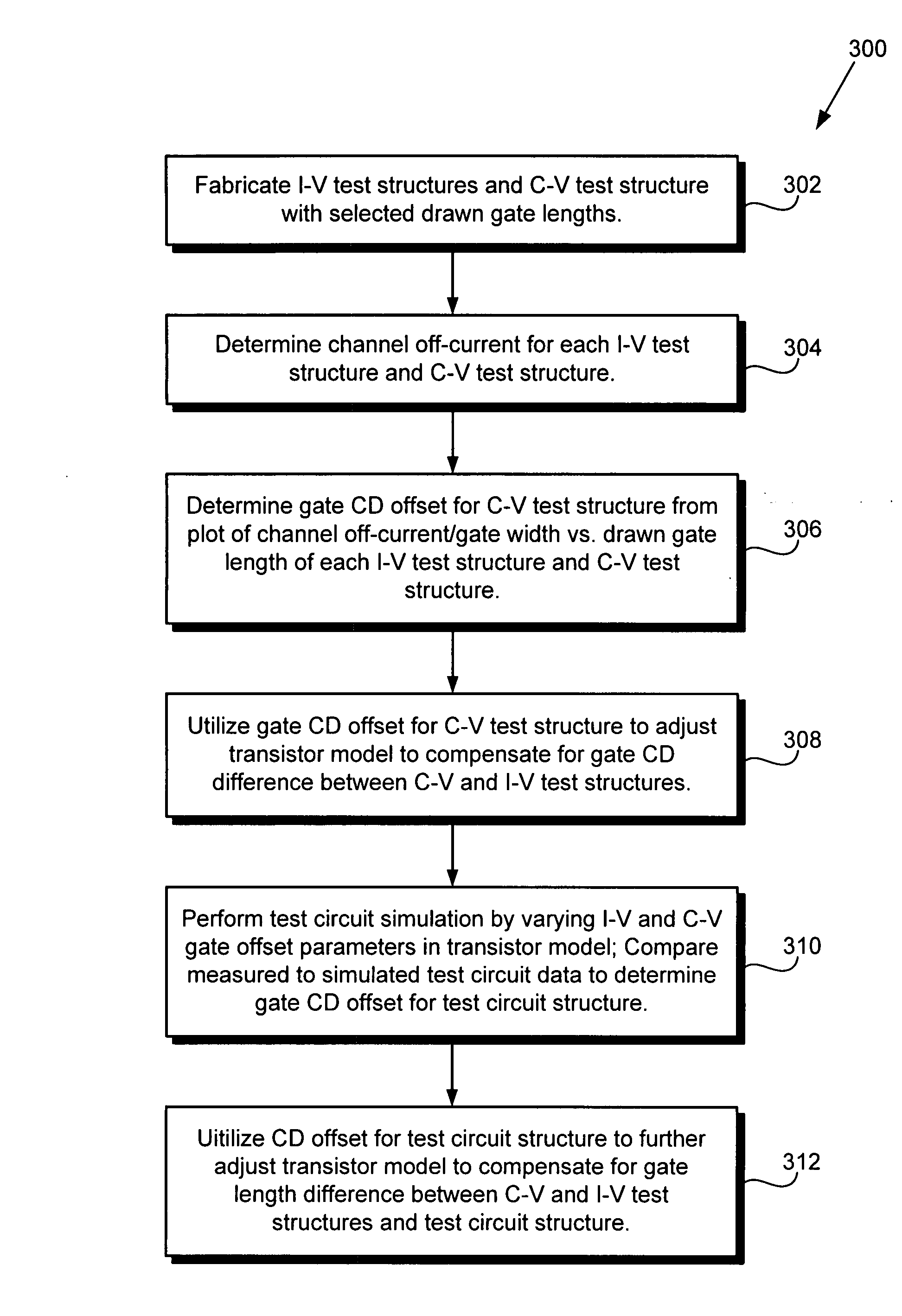
According to one exemplary embodiment, a method for adjusting a transistor model for increased circuit simulation accuracy includes determining a first gate CD offset by matching a C-V test structure having a normalized channel current to an I-V test structure having the normalized channel current. The method further includes utilizing the first gate CD offset to adjust the transistor model for increased circuit simulation. The method also includes determining a second gate CD offset by varying I-V and C-V gate length parameters in the transistor model to cause simulated data from a test circuit to be approximately equal to measured data from the test circuit. The method further includes utilizing the second gate CD offset to adjust the transistor model.

Description

TECHNICAL FIELD[0001]The present invention is generally in the field of semiconductor device modeling. More particularly, the invention is in the field of transistor modeling.BACKGROUND ART[0002]Transistor models, such as field effect transistor (FET) models, are critical in achieving reliable performance from circuit designs that include transistors. One significant purpose of a transistor model, such as a Metal-Oxide Semiconductor FET (MOSFET) model, is to verify circuit performance in simulation prior to actual fabrication of the circuit. The accuracy of a transistor model can be determined by how closely circuit simulation results, i.e., the predicted operation of the circuit, approximates circuit data measured from the fabricated circuit. For circuit simulation results to closely approximate measured circuit data, the transistor model requires accurate model parameters, such as current vs. voltage (I-V) and capacitance vs. voltage (C-V) model parameters.[0003]Transistor model p...

Claims


Application Information

Patent Timeline
Patent Type & Authority Applications(United States)
IPC IPC(8): H01L21/66G06F17/50
CPCG06F17/5036G06F30/367
Inventor GOO, JUNG-SUKCHEN, QIANG
Owner ADVANCED MICRO DEVICES INC
Learn More