Electronic component mounting system and electronic component mounting method

a technology for electronic components and mounting systems, applied in the direction of manufacturing tools, sustainable manufacturing/processing, final product manufacturing, etc., can solve the problems of inability to efficiently perform component mounting process and inability to use the position information of the soldering machine acquired by the print inspection apparatus

Active Publication Date: 2008-11-27
PANASONIC CORP
View PDF3 Cites 24 Cited by
  • Summary
  • Abstract
  • Description
  • Claims
  • Application Information

AI Technical Summary

Benefits of technology

[0029]According to the aspects of the invention, there is adopted a configuration in which solder position deviation data indicating the positional deviation of solder paste on each individual substrate is calculated for each individual substrate based on a mark position recognition result on a substrate recognition mark, a solder position recognition result on the printed solder paste, and electrode position information indicating the position of an electrode on each individual substrate, an operation of calculating position correction data, which is used to correct the positional deviation to mount electronic components at proper positions, is performed for each individual substrate based on the calculated solder position deviation data, and an electronic component mounting operation of the component mounting mechanism is controlled based on the mark position recognition result and the position correction data feed-forwarded in the electronic component mounting apparatus. As a result, mounting position correction in the component mounting form in which a plurality of individual substrates are held on a carrier can be efficiently performed.

Problems solved by technology

However, in the case when an inspection function of a known electronic component mounting line including the above-mentioned example in the related art is applied to such component mounting form in which a plurality of individual substrates are held on a carrier, the following problems occur.
For this reason, solder position information acquired by a print inspection apparatus could not be used and mounting position correction could not be efficiently performed in a component mounting process.

Method used


Image

  • Electronic component mounting system and electronic component mounting method
  • Electronic component mounting system and electronic component mounting method
  • Electronic component mounting system and electronic component mounting method

Examples


Embodiment Construction

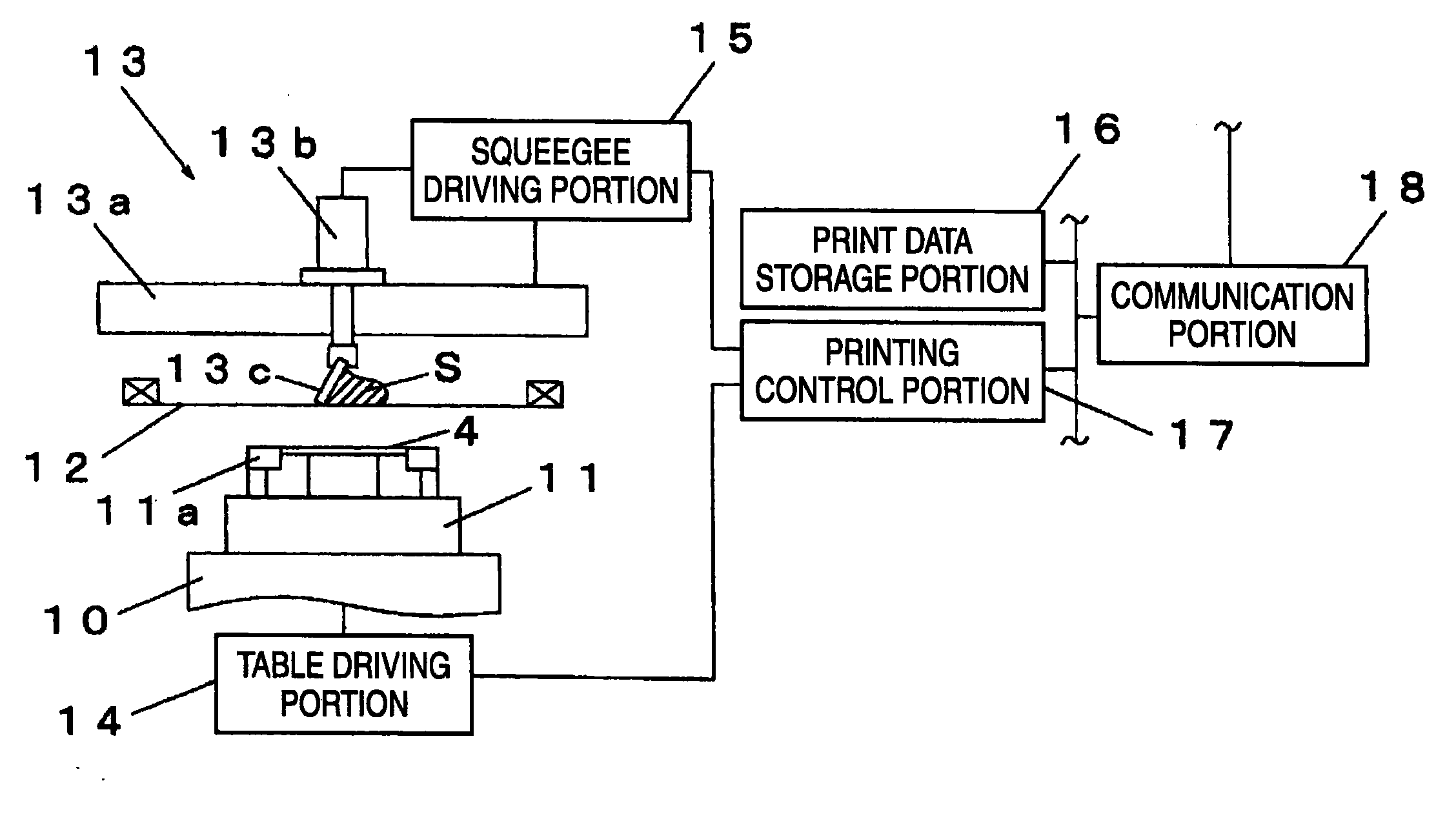
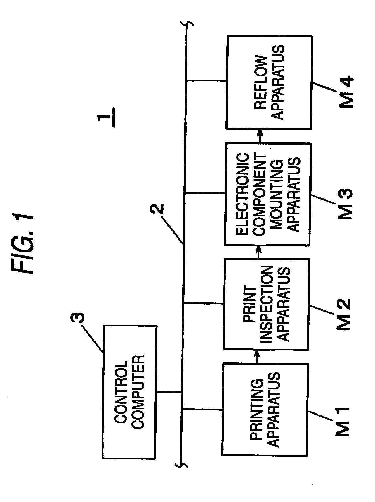
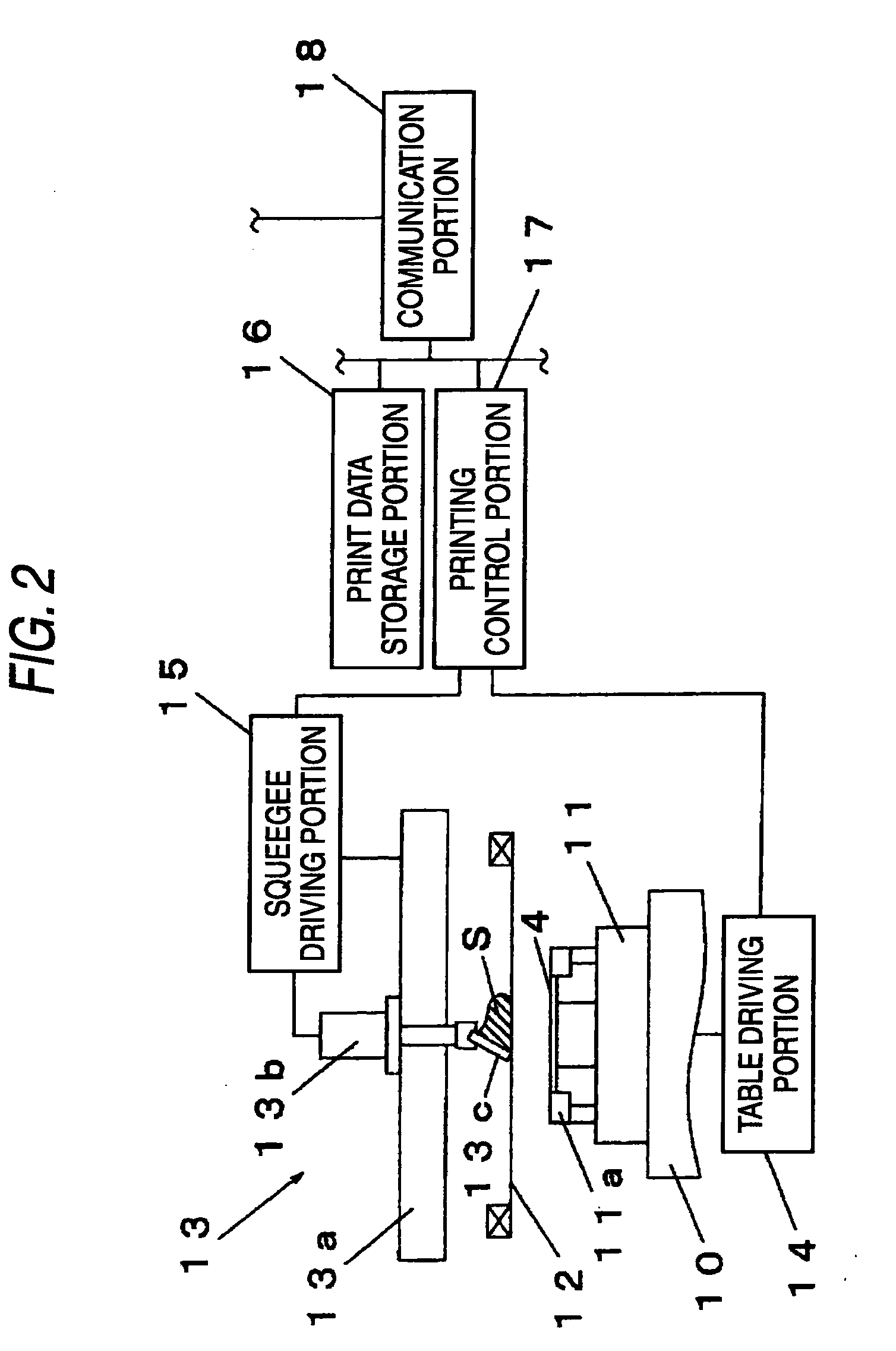
[0042]Hereinafter, embodiment of the invention will be described with reference to the accompanying drawings. FIG. 1 is a block diagram illustrating the configuration of an electronic component mounting system according to an embodiment of the invention. FIG. 2 is a block diagram illustrating the configuration of a printing apparatus in the electronic component mounting system according to the embodiment of the invention. FIG. 3 is a block diagram illustrating the configuration of a print inspection apparatus in the electronic component mounting system according to the embodiment of the invention. FIG. 4 is a block diagram illustrating the configuration of an electronic component mounting apparatus in the electronic component mounting system according to the embodiment of the invention. FIGS. 5A to 5C, 6A and 6B, 7A to 7C, and 8A and 8B are explanatory views illustrating the structures of targeted carrier and individual substrates in the electronic component mounting system accordin...


PUM

PropertyMeasurementUnit
structuresaaaaaaaaaa
shapeaaaaaaaaaa
sizeaaaaaaaaaa

Abstract

In electronic component mounting for a plurality of individual substrates held on a carrier, solder position deviation data is calculated for each individual substrate based on a mark position recognition result on a carrier after solder printing, a solder position recognition result, and electrode position information indicating the position of an electrode on each individual substrate, an operation of calculating position correction data, which is used to correct the positional deviation to mount electronic components at proper positions, is performed for each individual substrate based on the calculated solder position deviation data and the calculated position correction data is feed-forwarded to an electronic component mounting apparatus, and an electronic component mounting operation of a component mounting mechanism is controlled based on the mark position recognition result and the position correction data.

Description

BACKGROUND OF THE INVENTION[0001]1. Field of the Invention[0002]The present invention relates to an electronic component mounting system and an electronic component mounting method of mounting electronic components on a plurality of individual substrates held in a carrier by soldering to thereby manufacture an individual mounted board.[0003]2. Related Art[0004]An electronic component mounting system that mounts electronic components on a substrate by soldering to thereby manufacture a mounted board is formed by connecting a plurality of apparatuses for mounting of electronic components, such as a solder printing apparatus, an electronic component mounting apparatus, and a reflow apparatus. A technique for giving a function of automatically determining whether or not a component mounting operation has been properly performed by providing an inspection apparatus between apparatuses in order to perform quality control with high reliability in such an electronic component mounting syste...

Claims


Application Information

Patent Timeline
Patent Type & Authority Applications(United States)
IPC IPC(8): H05K3/34
CPCH01L23/544Y10T29/49144H01L24/83H01L2223/54426H01L2223/54473H01L2224/81121H01L2224/81801H01L2224/83121H01L2224/83801H05K1/0269H05K3/0097H05K3/1216H05K3/303H05K3/3484H05K2201/09918H05K2203/0165H05K2203/0545H05K2203/166H01L2924/01068H01L24/81Y10T29/49179Y10T29/49131Y10T29/53174Y10T29/53191Y10T29/53178H01L2924/3512H01L2924/00H05K3/3485Y02P70/50
Inventor INOUE, MASAFUMIKIKUTSUGI, FUMIOKIHARA, MASAHIRO
Owner PANASONIC CORP
Why Eureka
Try Eureka