Pattern designing method, pattern designing program and pattern designing apparatus
- Summary
- Abstract
- Description
- Claims
- Application Information
AI Technical Summary
Benefits of technology
Problems solved by technology
Method used
Image

Examples
first embodiment
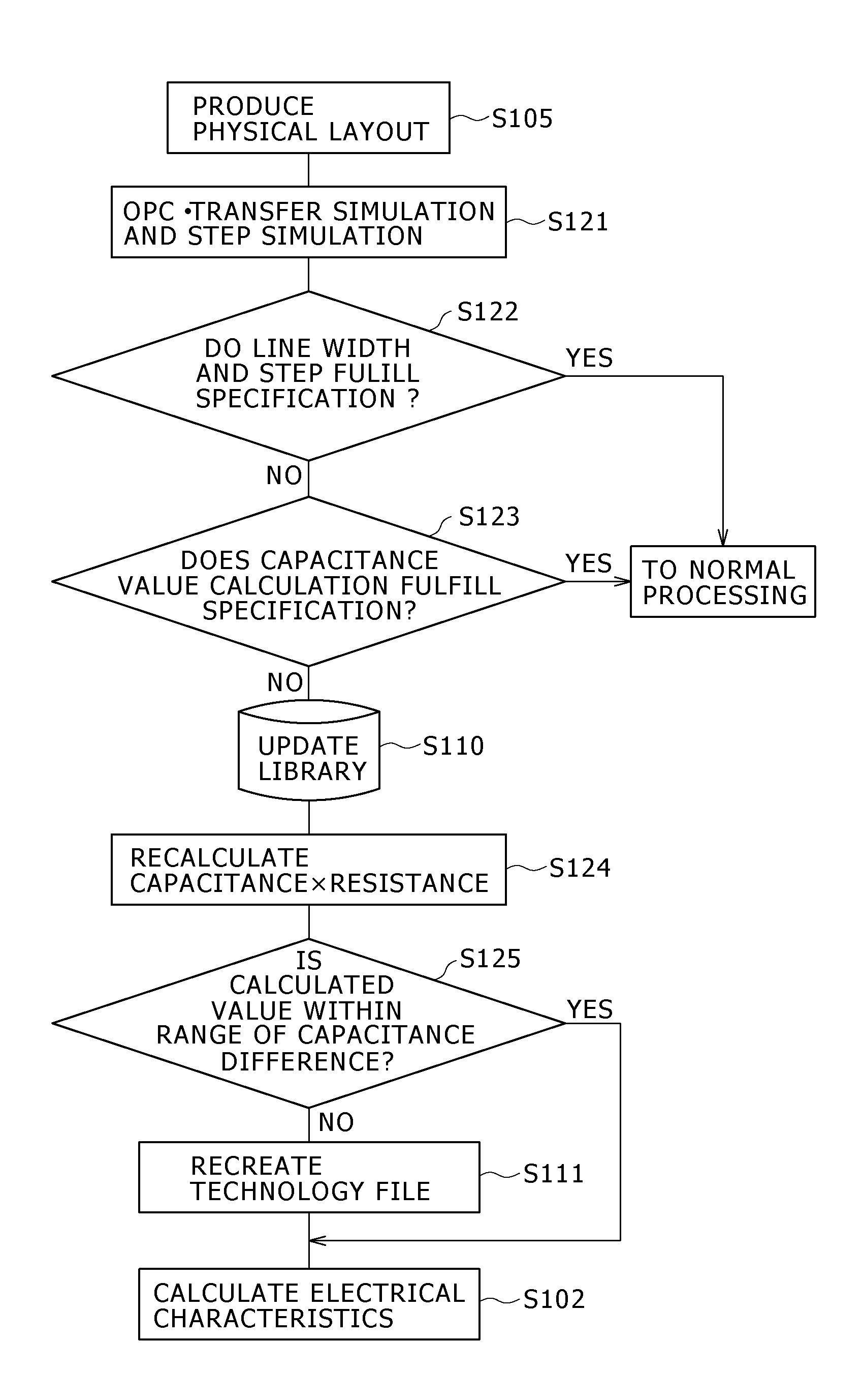
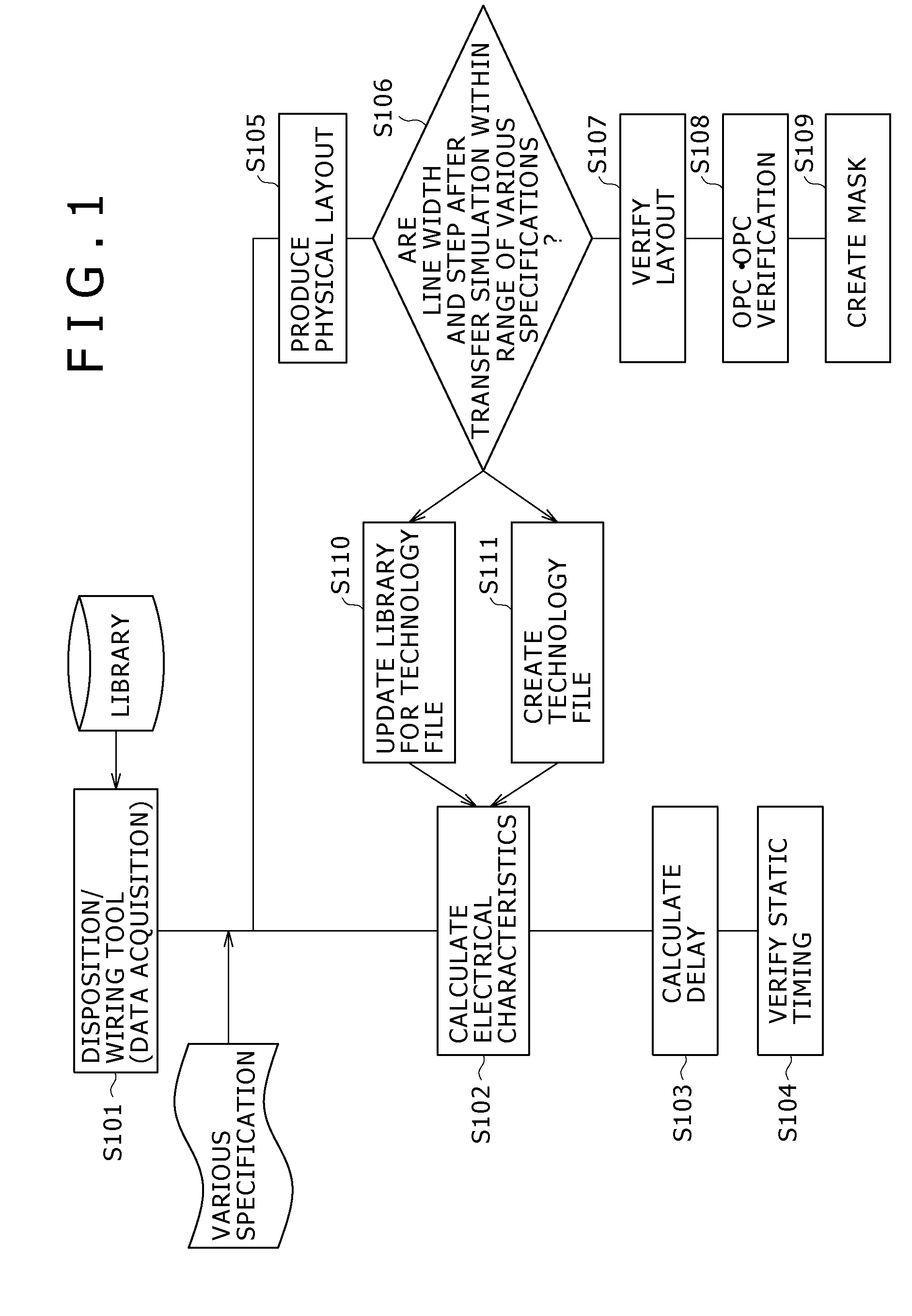
[0037]FIG. 1 is a flow chart explaining a flow of a pattern designing method according to a first embodiment of the present invention. In this pattern designing method, processing of Step S106, and Steps S110 and S111 as processing for a shape screening for a layout, and parameter inputting processing necessary for executing the processing described above are added to the same processing of Steps S101 to S104, Step S105, and Steps S107 to S109 as that in the related art pattern designing method shown in FIG. 8.
[0038]In addition, FIG. 2 is a flow chart showing the details of a main processing portion of the pattern designing method according to the first embodiment of the present invention. In FIG. 2, the same Step numbers, as those in FIG. 1, of Step numbers representing the processing shown in FIG. 2 represent the same processing as that in FIG. 1.
[0039]Hereinafter, the pattern designing method according to the first embodiment of the present invention will be described in detail w...
second embodiment
[0063]In a pattern designing method according to a second embodiment of the present invention, the processing of Steps in the described pattern designing method of the first embodiment is performed inside the disposition / wiring tool. FIGS. 5 and 6 show a flow of the pattern designing method according to the second embodiment of the present invention.
[0064]In Step S500 shown in FIG. 5, the various specifications are inputted to the disposition / wiring tool. The cell library, the technology file, the circuit connection information, and the like are normally inputted to the disposition / wiring tool. In addition thereto, the specifications about the dispersions in the line width and the thickness necessary for the shape screening, the typical cross-sectional structure of the device, the dispersion in the thickness of each of the layers, the difference for the capacitance value in the longitudinal structure of the typical device, and the like are also inputted to the disposition / wiring too...
third embodiment
[0076]A pattern designing method according to a third embodiment of the present invention aims at enhancing the precision necessary for an extraction method by combining a plurality of technology files each being created through the processing in the first or second embodiment.
[0077]With the general capacitance value extracting technique, the worst value and the best value are selected in a single uniform way with respect to the height, the width and the spacing of the wiring to be made the worst and best technology files, respectively. Also, the capacitance value extraction is carried out by using the two corners.
[0078]Here, the combination of the worst value and the best value as a result of changing the thicknesses of the metal and the interlayer films constituting the cross-sectional structure of the device in a single uniform way may be physically impossible. Therefore, it is thought to drive the corner in a borderline state too much.
[0079]Driving the corner in a borderline sta...
PUM
 Abstract
Description
Claims
Application Information
 - R&D Engineer
- R&D Manager
- IP Professional
- Industry Leading Data Capabilities
- Powerful AI technology
- Patent DNA Extraction
Browse by: Latest US Patents, China's latest patents, Technical Efficacy Thesaurus, Application Domain, Technology Topic.
© 2024 PatSnap. All rights reserved.Legal|Privacy policy|Modern Slavery Act Transparency Statement|Sitemap