Supercharge Your Innovation With Domain-Expert AI Agents!

Sensor package and method for fabricating the same

a sensor and package technology, applied in the field of semiconductor devices, can solve the problems of increasing fabrication time and cost, the present method still cannot meet the demand for thinner sensor packages, so as to reduce the difficulty of reducing the height of the whole sensor package, reduce the difficulty of manufacturing and cost, and simplify the manufacturing process

Inactive Publication Date: 2008-12-11
SILICONWARE PRECISION IND CO LTD
View PDF0 Cites 2 Cited by
  • Summary
  • Abstract
  • Description
  • Claims
  • Application Information

AI Technical Summary

Benefits of technology

The present invention provides a thinner sensor package and a method for fabricating it. The sensor package includes a substrate, a sensor chip, and a transparent cover. The sensor chip is bonded to the substrate through bonding wires, and the chip has a sensor region. An encapsulant is used to secure the chip in the opening of the substrate, and the transparent cover is attached to the substrate with an adhesive layer. The adhesive layer covers the bonding wires and the sensor region. The sensor chip is placed in the opening of the substrate instead of being stacked on top, which reduces the height of the sensor package. The invention also eliminates the need for conductive bumps, special substrates, and flip chip processes, simplifying the fabrication process and reducing cost.

Problems solved by technology

However, the dam structure 12 is required to have a height higher than height of the sensor chip 11 plus the bonding wires 10b such that the sensor chip 11 and the bonding wires 10b can be received in the space 12a. As a result, it becomes difficult to reduce height of the whole sensor package so as to meet demand for thinner sensor packages.
Thus, the present method still cannot meet demand for thinner sensor packages.
In addition, the transfer molding process of the present method increases the fabrication time and cost.
However, the flip-chip process, the process of forming conductive bumps on the glass plate, the special design of the circuit board with cavity as well as the use of additional conductive adhesive complicate the fabrication process, increase the fabrication cost and accordingly prevent practical application of the present method.
Therefore, how to provide a much thinner sensor package and method for fabricating the same that can overcome the above-described drawbacks has become urgent.

Method used


Image

  • Sensor package and method for fabricating the same
  • Sensor package and method for fabricating the same
  • Sensor package and method for fabricating the same

Examples


Embodiment Construction

[0024]The following illustrative embodiments are provided to illustrate the disclosure of the present invention, these and other advantages and effects can be apparent to those skilled in the art after reading the disclosure of this specification.

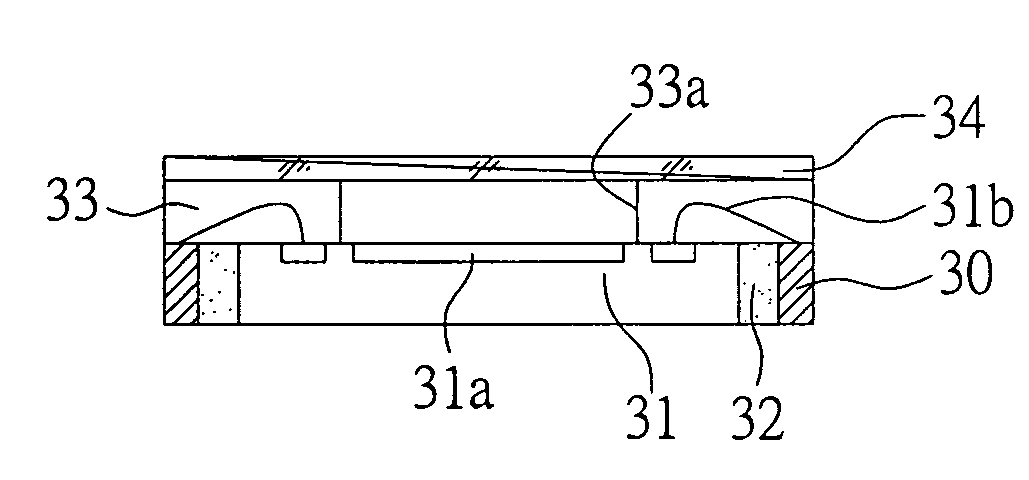
[0025]FIGS. 3A to 3E are diagrams showing a method for fabricating a sensor package according to a preferred embodiment of the present invention, wherein substrates, openings, sensor chips, bonding wires, encapsulant, film layers, and adhesive layers are only illustrative to disclose process steps and structural design and do not limit shape, size, or proportion thereof.

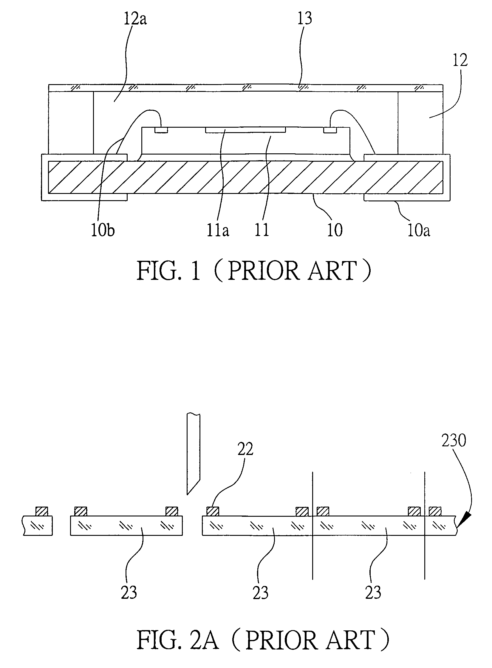
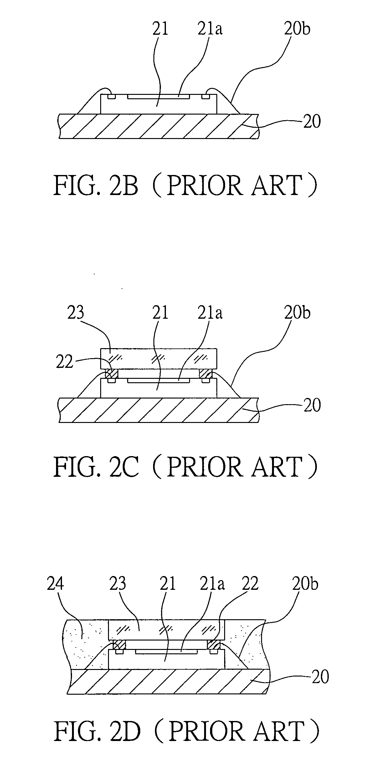
[0026]As shown in FIG. 3A, a substrate 30 having an opening 30a is provided and a film layer 30b is disposed at the bottom of the substrate 30 for sealing the bottom of the opening 30a. The film layer 30b will be removed in subsequent processes and there is no special limit to the film layer. In the present embodiment, the film layer 30b is a tape. In other embodiments, the ...


PUM


Abstract

The invention discloses a sensor package and a method for fabricating the same. The sensor package includes: a substrate with an opening; a sensor chip disposed in the opening and electrically connected to the substrate; an encapsulant filling spacing between the sensor chip and the opening so as to secure the sensor chip to the substrate; and a transparent cover attached to the substrate via an adhesive layer, wherein the adhesive layer covers the sensor chip and bonding wires and is formed with an opening for exposing sensor region of the sensor chip. Securing the sensor chip in the opening of the substrate reduces the height of the sensor package, and meanwhile the process cost is reduced by eliminating the need of formation of conductive bumps on the sensor chip or the transparent cover and eliminating the need of specially designed substrate.

Description

BACKGROUND OF THE INVENTION[0001]1. Field of the Invention[0002]The present invention relates generally to a semiconductor package and a method for fabricating the same, and more particularly to a sensor package having sensor chip and a method for fabricating the same.[0003]2. Description of Related Art[0004]In a conventional image sensor package, a sensor chip is mounted to a chip carrier and electrically connected to the chip carrier via bonding wires, and a glass cover is provided above the sensor chip so as to prevent water and dust from entering and meanwhile allow image light to be captured by the sensor chip. The image sensor package can be integrated to external devices such as printed circuit boards (PCBs) so as to be applied in various electronic products such as digital cameras, digital videos, optical mice, mobile phones, finger printer scanners and so on.[0005]FIG. 1 is a diagram showing a sensor package and a method for fabricating the same according to U.S. Pat. No. 6...

Claims


Application Information

Patent Timeline
Patent Type & Authority Applications(United States)
IPC IPC(8): H01L31/0203H01L31/18
CPCH01L23/24H01L31/0203H01L31/18H01L2224/32225H01L2224/48227H01L2224/73265H01L2224/48091H01L2924/00014H01L2924/00
Inventor CHAN, CHANG-YUEHHUANG, CHIEN-PINGCHANG, TSE-WENHUANG, CHIH-MINGHSIAO, CHENG-HSU
Owner SILICONWARE PRECISION IND CO LTD
Features
  • R&D
  • Intellectual Property
  • Life Sciences
  • Materials
  • Tech Scout
  • Unparalleled Data Quality
  • Higher Quality Content
  • 60% Fewer Hallucinations
Learn More