
Eureka
For R&D, Eureka makes reading and utilizing patents & technical documents easy.
Eureka AIR
Designed for self-driven R&D workflows. Generate viable solutions, solve complex R&D challenges, empower your innovation with AI.

Eureka Materials
Designed for material experts only. Revolutionize your material R&D, from search, analyze, to developing new materials.

TechResearch
Generate reliable direction feasibility study reports for your R&D in just a few steps.

TechSeek
Discover and master advanced knowledge NOW. Basics, ideas, possibilities, all at once.

TechMind
As an expert in R&D Theories, TechMind can generates customized viable solutions instantly.

TechRisk
Analyze your overall solution with one click, know your potential R&D risks in advance.

TechMonitor
Get weekly tech updates, stay abreast of the latest tech innovations and key insights.
Wiring substrate
- Summary
- Abstract
- Description
- Claims
- Application Information
AI Technical Summary
Benefits of technology
Problems solved by technology
Method used
Image

Examples
first embodiment
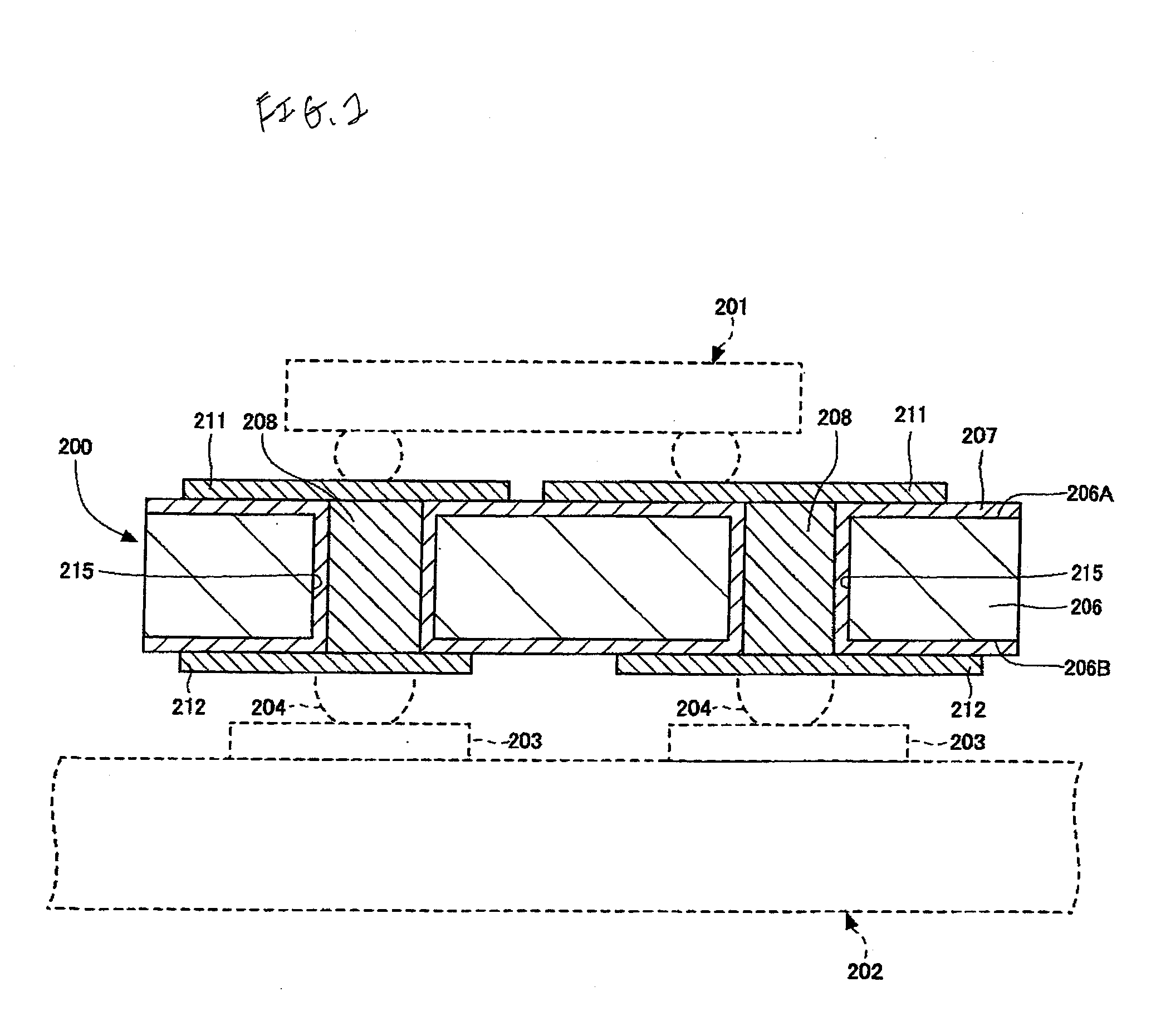
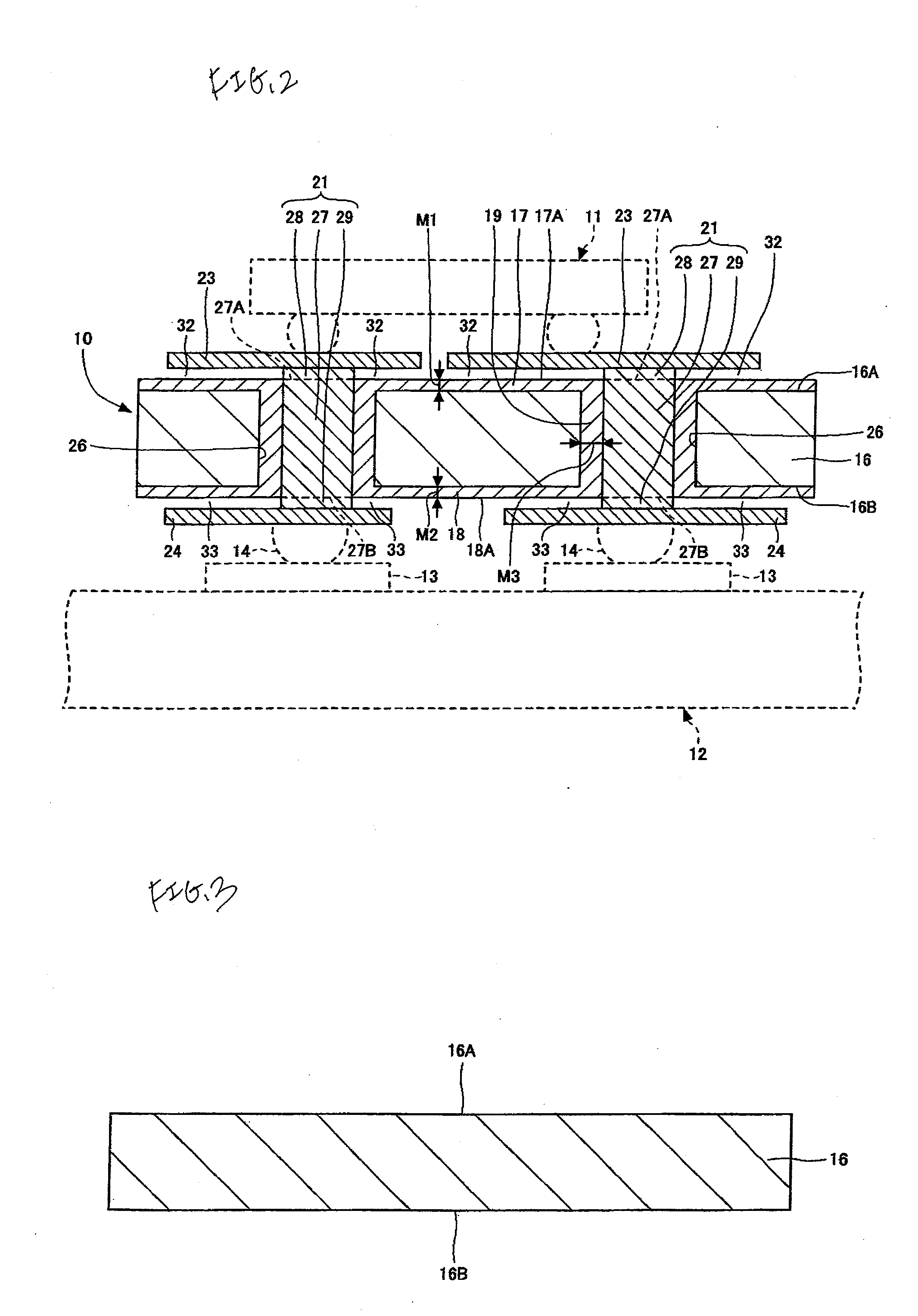
[0043]FIG. 2 is a sectional view of a wiring substrate according to a first embodiment of the present invention.
[0044]By reference to FIG. 2, a wiring substrate 10 of the first embodiment includes a semiconductor substrate 16, insulating films 17 to 19, through holes 21, first wiring patterns 23, and second wiring patterns 24.
[0045]The semiconductor substrate 16 is formed like a plate. The plurality of through holes 26 are formed in the semiconductor substrate 16. As the semiconductor substrate 16, a silicon substrate can be used, for example. When the silicon substrate is used as the semiconductor substrate 16, a thickness of the silicon substrate 16 can be set to 200 μm, for example.
[0046]The insulating film 16 is provided to cover an upper face 16A of the semiconductor substrate 16. When the silicon substrate is used as the semiconductor substrate 16, a thermal oxide film formed by thermally oxidizing the silicon substrate, for example, can be used as the insulating film 17. A th...
second embodiment
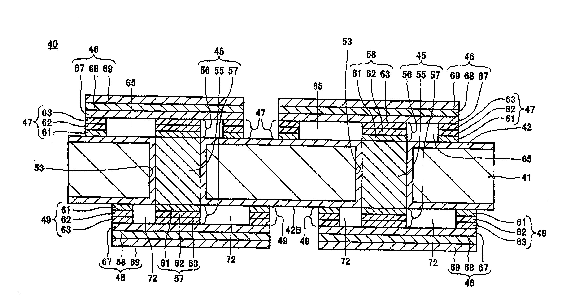
[0069]FIG. 9 is a sectional view of a wiring substrate according to a second embodiment of the present invention. In FIG. 9, the same reference symbols are affixed to the same constituent portions as those of the structure shown in FIG. 2.
[0070]By reference to FIG. 9, a wiring substrate 40 of the second embodiment includes a semiconductor substrate 41, an insulating film 42, through electrodes 45, first wiring patterns 46, first supporting members 47, second wiring patterns 48, and second supporting members 49.
[0071]The semiconductor substrate 41 is formed like a plate. Through holes 53 are formed in the semiconductor substrate 41. As the semiconductor substrate 41, a silicon substrate can be used, for example. When the silicon substrate is used as the semiconductor substrate 41, a thickness of the silicon substrate 41 can be set to 200 μm, for example.
[0072]The insulating film 42 is provided to cover an upper surface 41A of the semiconductor substrate 41, a lower surface 41B of the...
PUM
 Abstract
Description
Claims
Application Information
 - R&D Engineer
- R&D Manager
- IP Professional
- Industry Leading Data Capabilities
- Powerful AI technology
- Patent DNA Extraction
Browse by: Latest US Patents, China's latest patents, Technical Efficacy Thesaurus, Application Domain, Technology Topic, Popular Technical Reports.
© 2024 PatSnap. All rights reserved.Legal|Privacy policy|Modern Slavery Act Transparency Statement|Sitemap|About US| Contact US: help@patsnap.com