
Display substrate and liquid crystal display device having the same

a liquid crystal display and substrate technology, applied in non-linear optics, instruments, optics, etc., can solve problems such as uncoated areas, vertical alignment errors of alignment layers, and difficulty in forming alignment layers to have uniform thickness

Inactive Publication Date: 2008-12-25
SAMSUNG ELECTRONICS CO LTD
View PDF6 Cites 18 Cited by
  • Summary
  • Abstract
  • Description
  • Claims
  • Application Information

AI Technical Summary

Benefits of technology

The present invention provides a display substrate and a liquid crystal display device that can induce uniform liquid crystal alignment even when an inclined or protruding structure is formed on its surface. This allows for a more uniform and consistent liquid crystal layer alignment, resulting in improved display quality and response speed. The display substrate includes a common electrode, a cell gap maintaining part, a liquid crystal alignment support part, and an oxide alignment layer. The liquid crystal alignment support part has a plurality of inclined surfaces that pretilt the liquid crystal layer. The display device includes a first display substrate and a second display substrate with an oxide alignment layer and a liquid crystal layer between them. The invention prevents defects and improves the alignment speed and response speed of liquid crystal molecules.

Problems solved by technology

In the processes, a solution is coated on a transfer surface and then a solvent component is volatilized, so that it is difficult to form the alignment layers to have a uniform thickness when the process substrate has a non-flat structure.
For example, defects such as uncoated areas, vertical alignment errors of an alignment layer, etc. may be generated.
The vertical alignment errors are defects of which liquid crystal molecules are laid along two end portions of an inclined structure or an inclined portion.

Method used


Image

  • Display substrate and liquid crystal display device having the same
  • Display substrate and liquid crystal display device having the same
  • Display substrate and liquid crystal display device having the same

Examples


Embodiment Construction

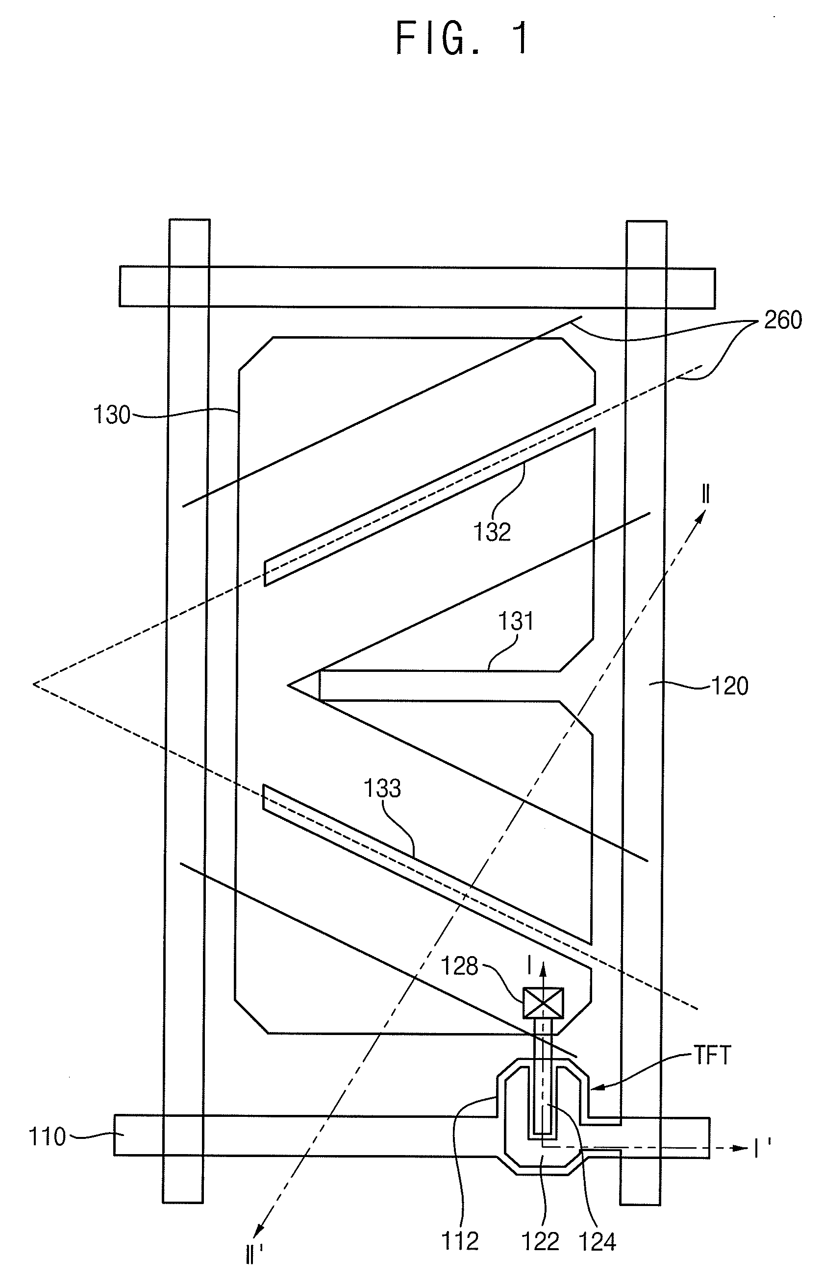
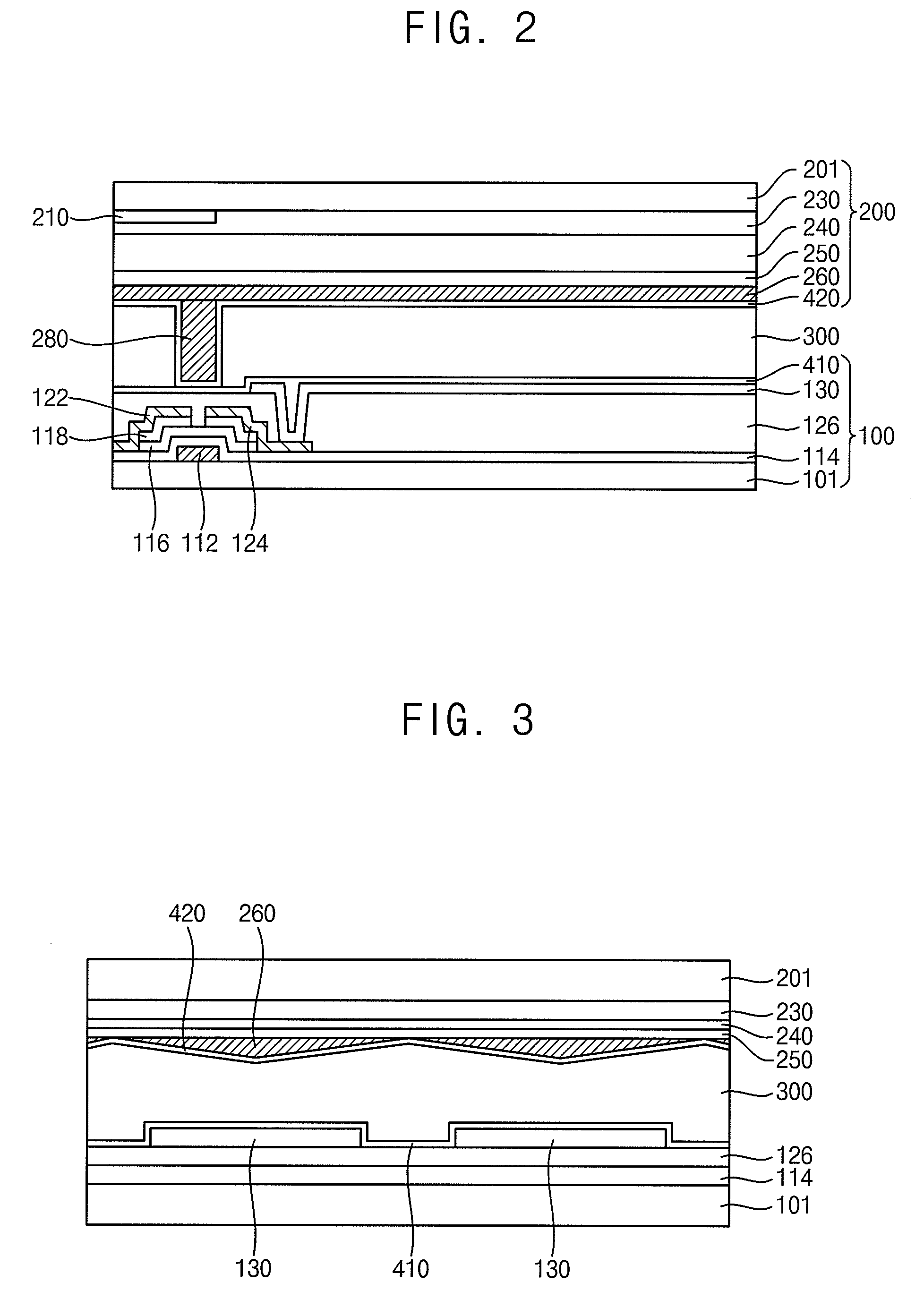
[0029]FIG. 1 is a plan view of a multi-domain liquid crystal display (“LCD”) device according to an exemplary embodiment of the present invention. FIG. 2 is a cross-sectional view taken along section line I-I′ of FIG. 1. FIG. 3 is a cross-sectional view taken along section line II-II′ of FIG. 1.

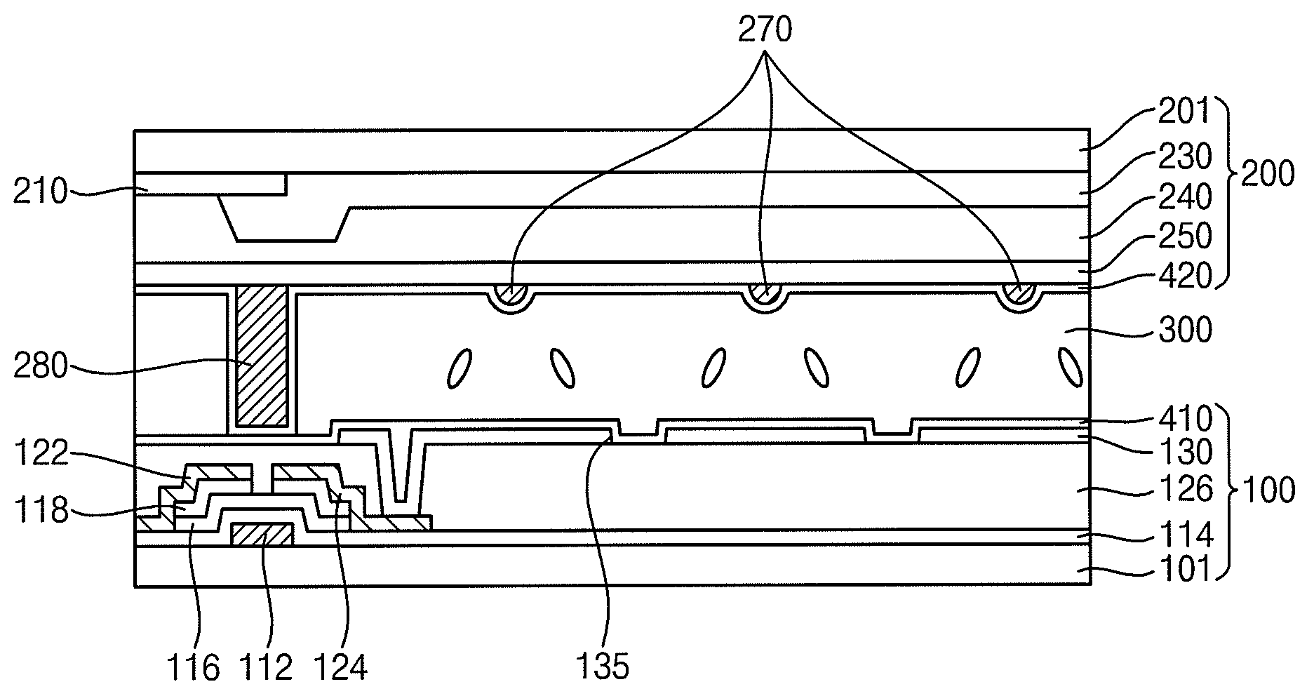
[0030]Referring to FIGS. 1 to 3, an LCD device according to an exemplary embodiment of the present invention includes a first display substrate 100, a second display substrate 200 and a liquid crystal layer 300 interposed between the first and second substrates 100 and 200.

[0031]The first display substrate 100 includes a first insulation substrate 101, a plurality of gate lines 110 that extends in a first direction on the first insulation substrate 101, a plurality of data lines 120 perpendicular to and crossing the gate lines 110, and a plurality of pixel electrodes 130. A charge developed on each pixel electrode 130 depends upon voltages on one of the gate lines 110 and one of the data line...


PUM

PropertyMeasurementUnit
pretilt anglesaaaaaaaaaa
Dielectric constantsaaaaaaaaaa

Abstract

A display substrate includes an insulation substrate, a common electrode, a cell gap maintaining part, a liquid crystal (LC) alignment support part and an oxide alignment layer. The common electrode is formed on the insulation substrate. The cell gap maintaining part is formed on the common electrode. The LC alignment support part of an organic material is formed on the common electrode. The oxide alignment layer is formed on the LC alignment support part. Therefore, the alignment speed and response speed of liquid crystal molecules may be enhanced.

Description

CROSS-REFERENCE TO RELATED APPLICATIONS[0001]This application claims priority under 35 U.S.C. § 119, of Korean Patent Application No. 2007-61080, filed on Jun. 21, 2007 in the Korean Intellectual Property Office (KIPO), which is herein incorporated by reference in its entirety.BACKGROUND OF THE INVENTION[0002]1. Field of the Invention[0003]The present invention relates to a display substrate and a liquid crystal display (“LCD”) device having the display substrate. More particularly, the present invention relates to a display substrate capable of enhancing an alignment speed and response speed of liquid crystal molecules, and an LCD device having the display substrate.[0004]2. Description of the Related Art[0005]Generally, a liquid crystal display (“LCD”) device includes an array substrate, a color filter substrate and a liquid crystal layer. The liquid crystal layer including a plurality of liquid crystal molecules is interposed between the array substrate and the color filter subst...

Claims


Application Information

Patent Timeline
Patent Type & Authority Applications(United States)
IPC IPC(8): G02F1/1337
CPCG02F1/133707G02F1/1337
Inventor JUNG, MIN-SIKRHO, SOON-JOONJEON, BAEK-KYUNLEE, HEE-KEUN
Owner SAMSUNG ELECTRONICS CO LTD
Learn More