Liquid crystal display panel and device

A liquid crystal display panel and liquid crystal display device technology, which is applied in static indicators, nonlinear optics, instruments, etc., can solve the problems of difficult control of deep and shallow hole resistance precision, uneven voltage, uneven optical alignment and alignment, etc., to improve the display effect , avoid the effect of uneven voltage and uniform alignment

Active Publication Date: 2017-06-09
SHENZHEN CHINA STAR OPTOELECTRONICS TECH CO LTD
View PDF9 Cites 6 Cited by
  • Summary
  • Abstract
  • Description
  • Claims
  • Application Information

AI Technical Summary

Problems solved by technology

[0006] However, in the actual manufacturing process, due to the influence of film thickness, exposure, etching and other aspects, it is difficult to control the internal resistance of T3 and the resistance accuracy of deep and shallow holes.
That is to say, the internal resistance of T3 and the resistance of the deep and shallow holes tend to fluctuate, resulting in uneven voltage of the sub-pixel portion 102, which easily leads to uneven alignment during optical alignment, which reduces the display effect

Method used


Image

  • Liquid crystal display panel and device
  • Liquid crystal display panel and device
  • Liquid crystal display panel and device

Examples


Embodiment Construction

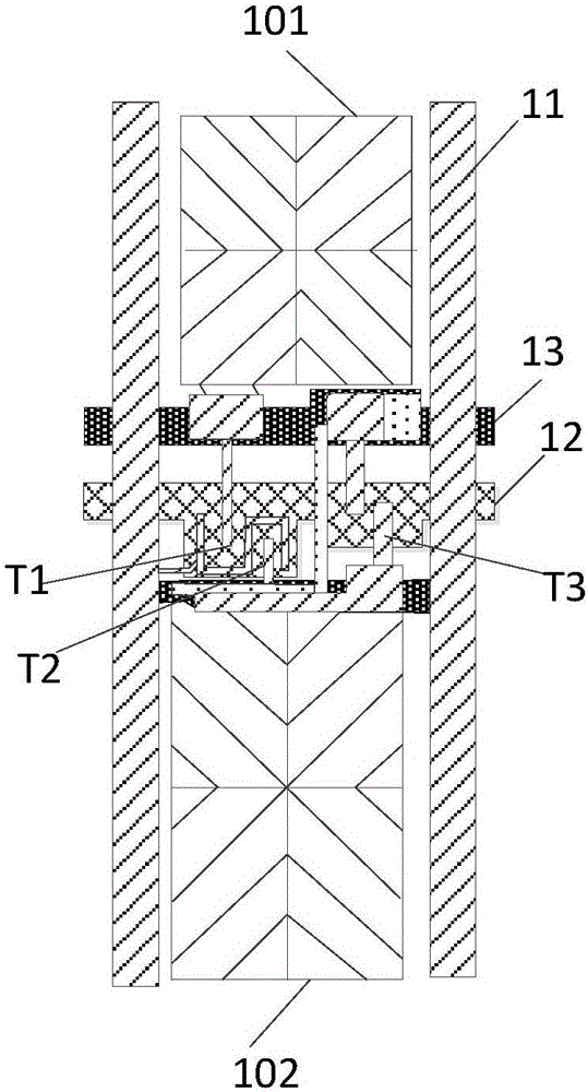
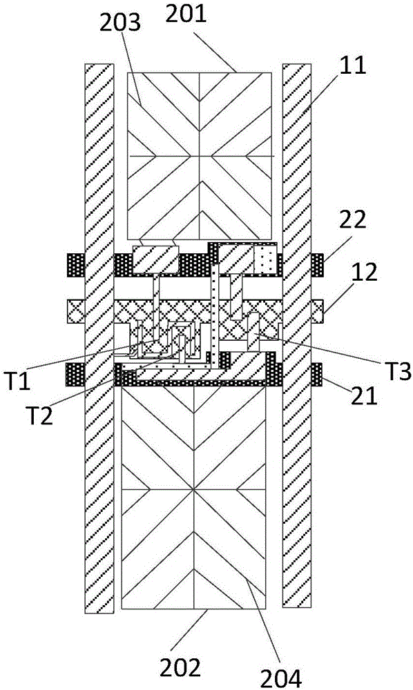
[0029] The following descriptions of the various embodiments refer to the accompanying drawings to illustrate specific embodiments in which the present invention can be practiced. The directional terms mentioned in the present invention, such as "up", "down", "front", "back", "left", "right", "inside", "outside", "side", etc., are for reference only The orientation of the attached schema. Therefore, the directional terms used are used to illustrate and understand the present invention, but not to limit the present invention. In the figures, structurally similar units are denoted by the same reference numerals.

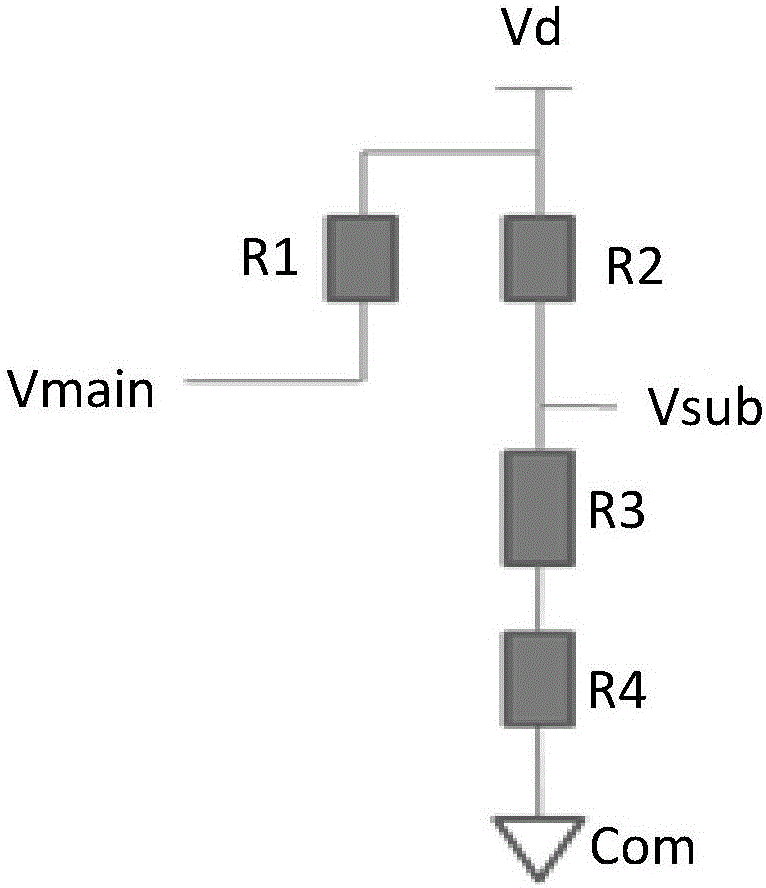
[0030] Please refer to figure 2 , figure 2 It is an equivalent circuit diagram of an existing liquid crystal display panel.

[0031] Such as figure 2 As shown, the electrical principle of the existing liquid crystal display panel is specifically as follows: when the scanning line 12 is turned on, T2 and T3 are turned on, and its internal resistance and deep and...


PUM


Abstract

The invention provides a liquid crystal display panel and a liquid crystal display device. The liquid crystal display panel comprises a data line, a scanning line, a first common line, a second common line, a main pixel part and a sub-pixel part; the first common line is used for providing a common voltage; the second common line is used for making the voltage of the sub-pixel part equal to a fixed value when the liquid crystal display panel is aligned; the voltage of the main pixel part is not equal to the voltage of the sub-pixel part. According to the liquid crystal display panel and the liquid crystal display device, provided by the invention, the display effect is improved.

Description

[0001] 【Technical field】 [0002] The invention relates to the technical field of displays, in particular to a liquid crystal display panel and a device. [0003] 【Background technique】 [0004] With the improvement of the fineness of the liquid crystal display panel, the size of the pixel becomes smaller and smaller, and the aperture ratio of the pixel also becomes smaller, thereby affecting the display brightness. [0005] In order to increase display brightness, such as figure 1 As shown, the existing display panel includes a main pixel portion 101 and a sub-pixel portion 102, and three thin film transistors T1-T3, the gates of T1-T3 are connected to the scanning line 12, and the sources of T1 and T2 are connected to the data line 11 connection, the source of T3 is connected to the common line 13 through deep and shallow holes. The internal resistance of T3 is much smaller than that of T2, and the size of T3 is smaller than that of T2. The potential of the sub-pixel part ...

Claims


Application Information

Patent Timeline
Patent Type & Authority Applications(China)
IPC IPC(8): G02F1/1337G02F1/1362
CPCG02F1/133707G02F1/136286G02F1/13624G09G3/3648G09G2300/0426G09G2300/0447G09G2320/0223G02F1/134345
Inventor 姜祥卫
Owner SHENZHEN CHINA STAR OPTOELECTRONICS TECH CO LTD
Why Eureka
Try Eureka