Optical device, exposure apparatus, and device manufacturing method
- Summary
- Abstract
- Description
- Claims
- Application Information
AI Technical Summary
Benefits of technology
Problems solved by technology
Method used
Image
Examples
first embodiment
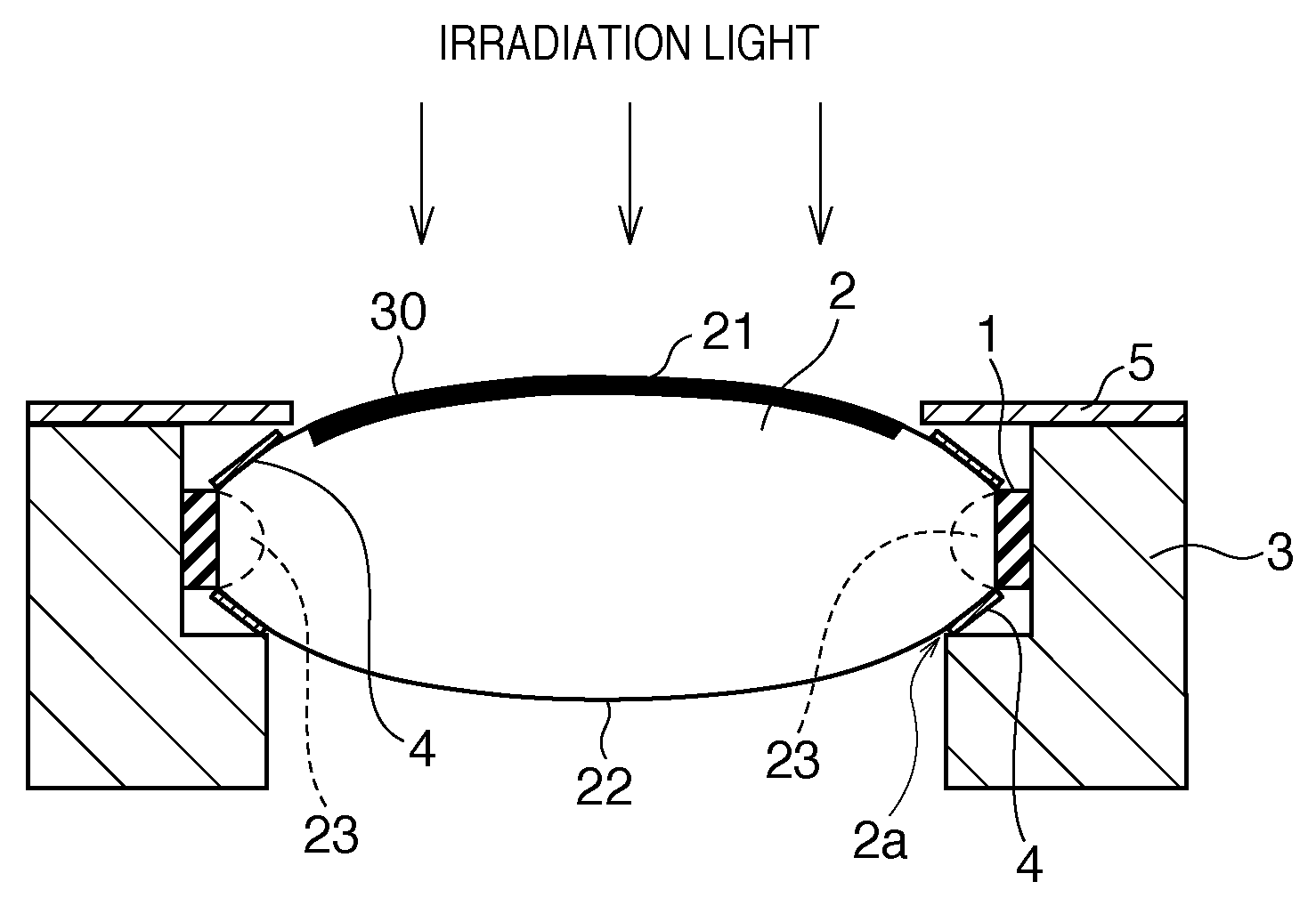
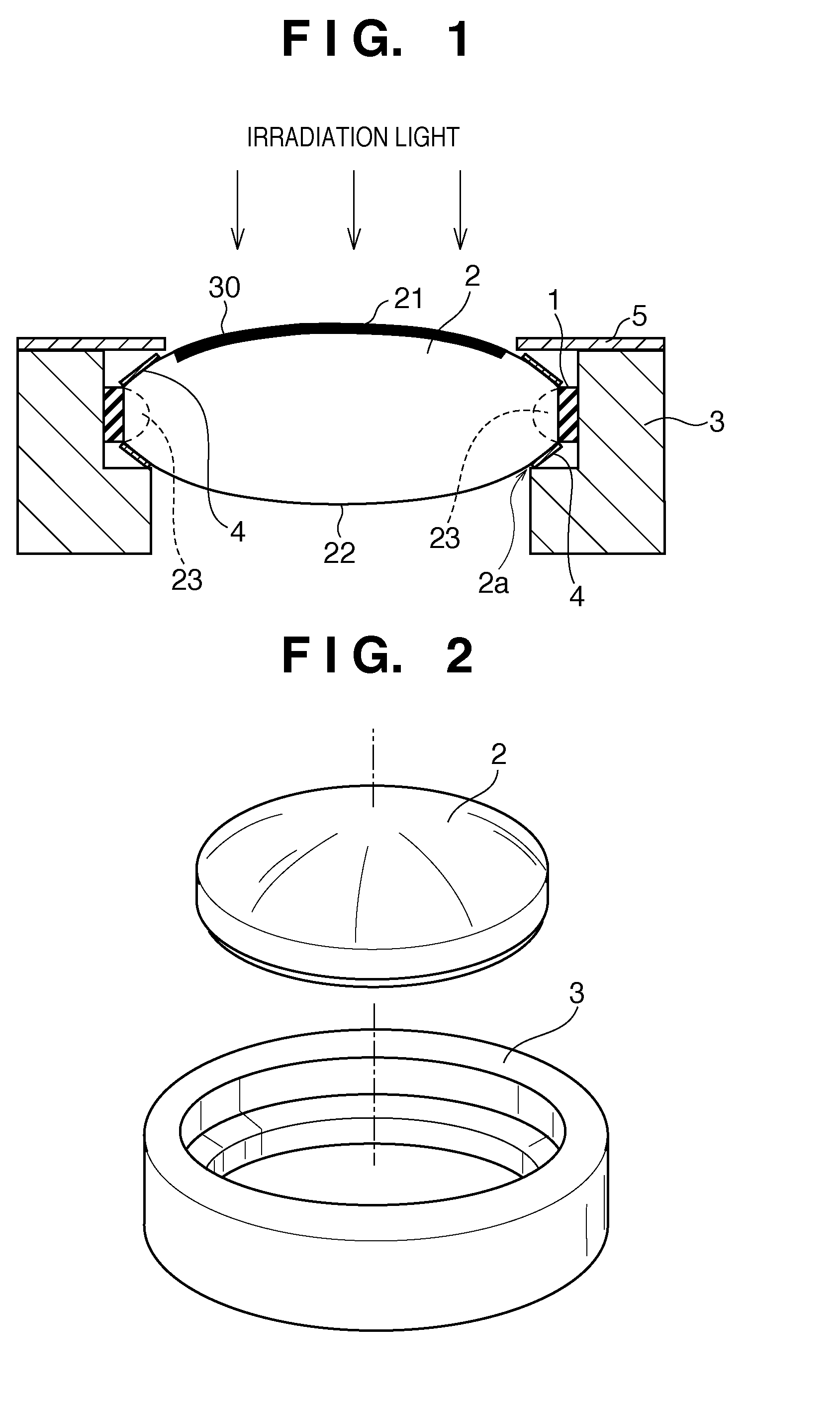
[0020]FIG. 1 shows the schematic arrangement of an optical device according to the first embodiment of the present invention. The optical device according to the first embodiment comprises an optical element 2, a supporting member 3 which is connected to a part 23 of the optical element 2 through an adhesive material 1 and supports the optical element 2, and a light shielding film 4 formed on the surface of the optical element 2 to limit light incidence on the adhesive material 1.
[0021]An example of the optical element 2 is a lens. The part 23 of the optical element 2 is typically at least a part of the side portion of the optical element 2. The light shielding film 4 can be formed on the surface of the optical element 2 by, e.g., coating. Referring to FIG. 1, irradiation light enters the optical element 2 from its upper surface side (to be referred to as an object side hereinafter). The irradiation light irradiates an irradiated region 30 on an object side surface 21 of the optical...
second embodiment
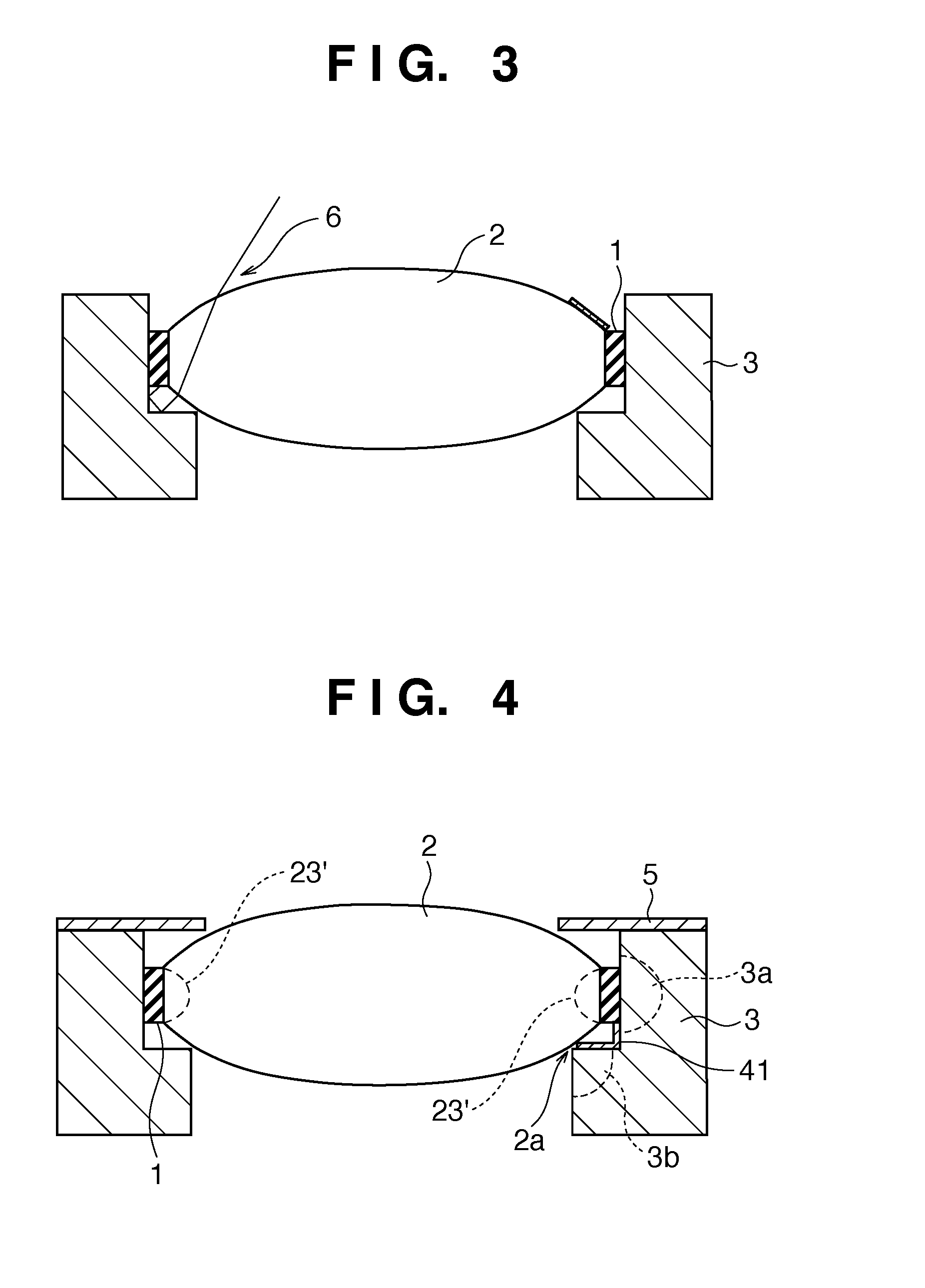
[0026]FIG. 4 shows the schematic arrangement of an optical device according to the second embodiment of the present invention. The optical device according to the second embodiment comprises an optical element 2, a supporting member 3 which is connected to at least a part 23′ of the side portion of the optical element 2 through an adhesive material 1 and supports the optical element 2, and an incidence limiting portion 41 which limits light incidence on the adhesive material 1. An example of the optical element 2 is a lens.
[0027]The supporting member 3 comprises a first supporting portion 3a which is connected to at least the part 23′ of the side portion of the optical element2 through the adhesive material 1, and a second supporting portion 3b which supports the peripheral portion of the optical element 2 from below. The incidence limiting portion 41 is inserted between the contact portion between the adhesive material 1 and the first supporting portion 3a and a contact portion 2a ...
third embodiment
[0029]FIG. 5 shows the schematic arrangement of an optical device according to the third embodiment of the present invention. The third embodiment is different from the second embodiment in that an incidence limiting portion 41 is additionally provided on a side opposite to a second supporting portion 3b with respect to an adhesive material 1. A description of the same parts as those in the above-described embodiments will not be repeated. As shown in FIG. 5, a light beam 61 which has been generated by scattered light and has entered an optical element 2 can enter the adhesive material 1 upon being reflected by an image side surface 22 of the optical element 2 and further reflected by a light shielding member 5. To avoid this situation, the incidence limiting portions 41 are provided on the surface of the light shielding member 5 on the side of the adhesive material 1 and on the surface of a supporting member 3 from the adhesive material 1 to the light shielding member 5, as shown i...
PUM
 Abstract
Description
Claims
Application Information


