Rd Algorithm Improvement for Nrom Technology

a technology of rd algorithm and nrom, which is applied in the direction of read-only memories, instruments, and static storage, etc., can solve the problems of loss of anything contained in ram, voltage drift is especially problematic, and corruption of data in memory array, etc., and achieve the effect of enlarging or restricting the channel, enabling the change of channel conductivity and reducing the loss of ram

Inactive Publication Date: 2009-01-01
SPANSION ISRAEL
View PDF28 Cites 46 Cited by
  • Summary
  • Abstract
  • Description
  • Claims
  • Application Information

AI Technical Summary

Benefits of technology

[0003]The transistor is a solid state semiconductor device which can be used for amplification, switching, voltage stabilization, signal modulation and many other functions. Generally, a transistor has three terminals, and a voltage applied to a specific one of the terminals controls current flowing between the other two terminals.
[0004]The terminals of a field effect transistor (FET) are commonly named source, gate and drain. In the FET a small amount of voltage is applied to the gate in order to control current flowing between the source and drain. In FETs the main current appears in a narrow conducting channel formed near (usually primarily under) the gate. This channel connects electrons from the source terminal to the drain terminal. The channel conductivity can be altered by varying the voltage applied to the gate terminal, enlarging or constricting the channel and thereby controlling the current flowing between the source and the drain.
[0005]FIG. 1 illustrates a FET 100 comprising a p-type substrate, and two spaced-apart n-type diffusion areas—one of which will serve as the “source”, the other of which will serve as the “drain” of the transistor. The space between the two diffusion areas is the “channel”. A thin dielectric layer is disposed over the substrate in the neighborhood of the channel, and a “gate” structure is disposed over the dielectric layer atop the channel. (The dielectric under the gate is also commonly referred to as “gate oxide” or “gate dielectric”.) Electrical connections (not shown) may be made to the source, the drain, and the gate. The substrate may be grounded.
[0006]Generally, when there is no voltage on the gate, there is no electrical conduction (connection) between the source and the drain. As voltage (of the correct polarity) is applied to the gate, there is a “field effect” in the channel between the source and the drain, and current can flow between the source and the drain, and can be controlled by the voltage applied to the gate. In this manner, a small signal (gate voltage) can control a relatively large signal (current flow between the source and the drain).
[0007]A floating gate transistor is generally a transistor structure, broadly based on the FET, as described hereinabove. As illustrated in FIG. 2, the floating gate transistor 200 has a source and a drain, but rather than having only one gate, it has two gates which are called control gate (CG) and floating gate (FG). It is this arrangement of control gate and floating gate which enables the floating gate transistor to function as a memory cell, as described hereinbelow.
[0008]The floating gate is disposed over tunnel oxide (comparable to the gate oxide of the FET). The floating gate is a conductor, the tunnel oxide is an insulator (dielectric material). Another layer of oxide (interpoly oxide, also a dielectric material) separates the floating gate from the control gate.

Problems solved by technology

These variations may occur due to charge leakage from the cell's charge storage region, temperature changes, and due to interference from the operation of neighboring NVM cells.
Variation of the threshold voltage of memory cells may lead to false reads of the cell's state and may further result in the corruption of the data in the memory array.
Voltage drift is especially problematic in MLC cells (see FIG. 5A) where the Vt regions or sub-ranges associated with each programmed state are relatively smaller than those for a typical binary or SLC cell (see FIG. 5B).
The most widely used form of primary storage today is a volatile form of random access memory (RAM), meaning that when the computer is shut down, anything contained in RAM is lost.
Unfortunately most forms of non-volatile memory have limitations which make it unsuitable for use as primary storage.
Typically non-volatile memory either costs more or performs worse than volatile random access memory.
In contrast, other types of memory devices (such as magnetic tapes, disks, and drums) can access data on the storage medium only in a predetermined order due to constraints in their mechanical design.

Method used


Image

  • Rd Algorithm Improvement for Nrom Technology
  • Rd Algorithm Improvement for Nrom Technology
  • Rd Algorithm Improvement for Nrom Technology

Examples


Embodiment Construction

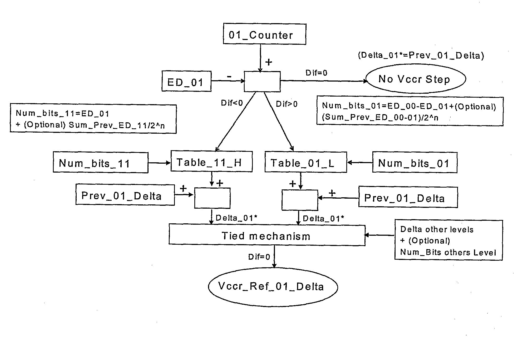
[0189]Generally, when reading memory cells, the correct read value (RV) should be such that all of the cells programmed to a Vt higher than RV (this should include all of the cells programmed to 00 and 01) should actually have a Vt that is higher than RV. For example, with reference to FIG. 5B,[0190]all of the cells programmed to 01, 00 and 10 should have a threshold voltage higher than RV01,[0191]all of the cells programmed to 00 and 10 should have a threshold voltage higher than RV00, and[0192]all of the cells programmed to 10 should have a threshold voltage higher than RV10.

[0193]Then, for example, by subtracting out the number of cells having a threshold voltage above RV10 (which should include only the cells programmed to 01), the number of cells programmed to 00 can be determined.

[0194]Using error detection (ED) techniques, the number of cells programmed at each program level is known (it may be counted before or during programming). For example, if 512 cells (or storage areas...


PUM


Abstract

Selecting a read voltage level for a NVM cell by using an initial value for the read voltage and performing a read operation, comparing an actual number of bits found to an expected number of bits and, if there is a discrepancy between the actual number and the expected number, adjusting the read voltage level, based on variable data such as statistics available, level occupation, neighbor level, previous chunks data, and other data used during read, program or erase. For example, based on a number of missing bits, or upon a result of a previous read operation, or a result obtained at another program level, or upon how many times the memory cell has been cycled, or upon how many memory cells are at each program level, or on a number of bits at another program level in a selected chunk of memory.

Description

CROSS-REFERENCE TO RELATED APPLICATIONS[0001]This application claims the benefit of U.S. Provisional Application No. 60 / 757,468, filed Jan. 10, 2006, the entire disclosure of which is incorporated herein by reference.TECHNICAL FIELD[0002]The disclosure relates to the field of non-volatile memory (“NVM”) cells and, more particularly, to a technique for selecting a reference voltage for reading the state of the memory cells.BACKGROUNDThe Field Effect Transistor[0003]The transistor is a solid state semiconductor device which can be used for amplification, switching, voltage stabilization, signal modulation and many other functions. Generally, a transistor has three terminals, and a voltage applied to a specific one of the terminals controls current flowing between the other two terminals.[0004]The terminals of a field effect transistor (FET) are commonly named source, gate and drain. In the FET a small amount of voltage is applied to the gate in order to control current flowing between...

Claims


Application Information

Patent Timeline
Patent Type & Authority Applications(United States)
IPC IPC(8): G11C16/06G11C7/00
CPCG11C16/26G11C16/0475
Inventor RIZEL, ARIKCOHEN, GUY
Owner SPANSION ISRAEL
Why Eureka
Try Eureka