
Electrical device to mask systematic luminance variation

a technology of luminance variation and electric device, which is applied in the field of electric devices, can solve the problems of small but noticeable variations in luminance uniformity, and reduce and achieve the effect of reducing the quality threshold for acceptable quality display devices and easy detection

Active Publication Date: 2017-05-18
LG CHEM LTD
View PDF0 Cites 1 Cited by
  • Summary
  • Abstract
  • Description
  • Claims
  • Application Information

AI Technical Summary

Benefits of technology

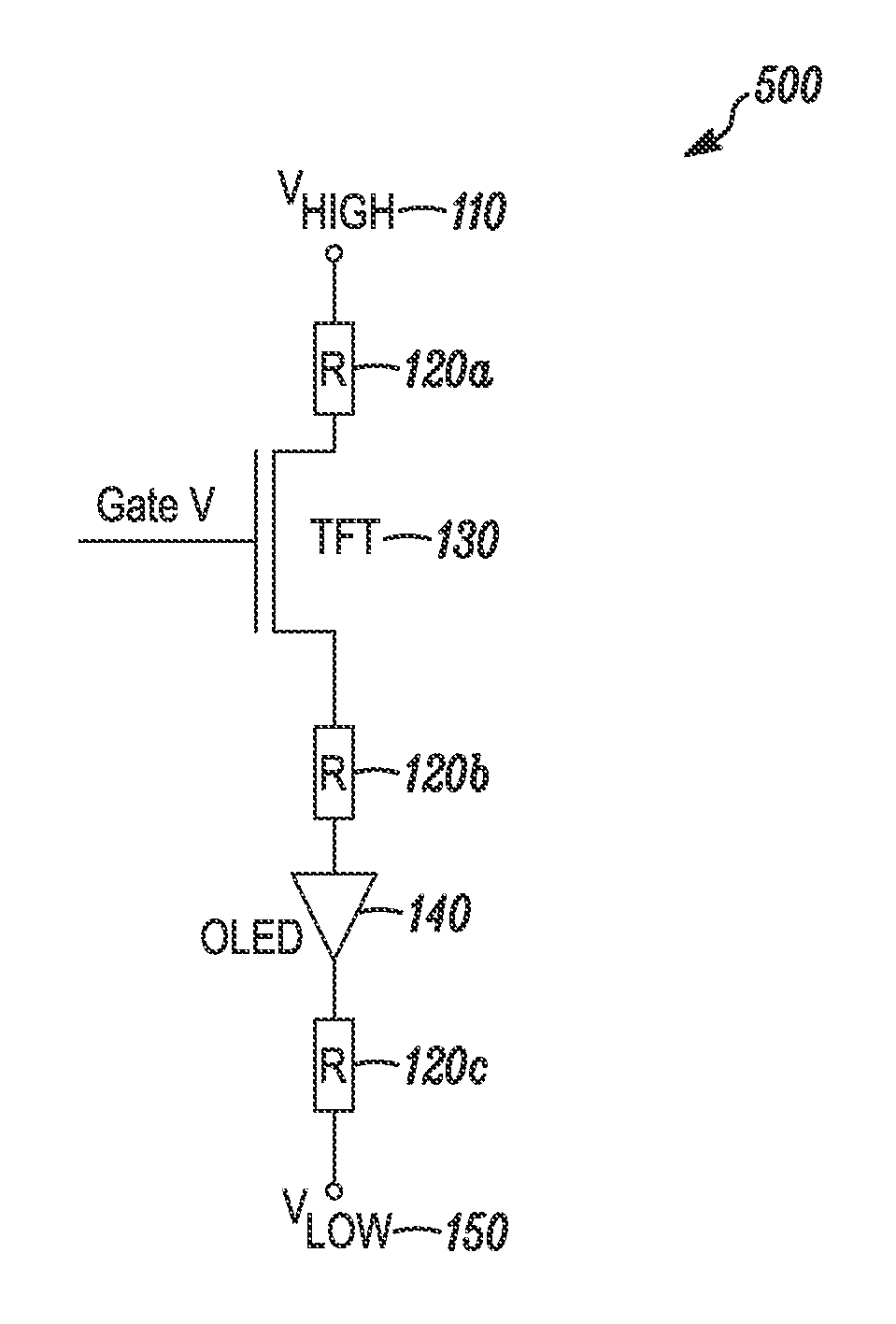
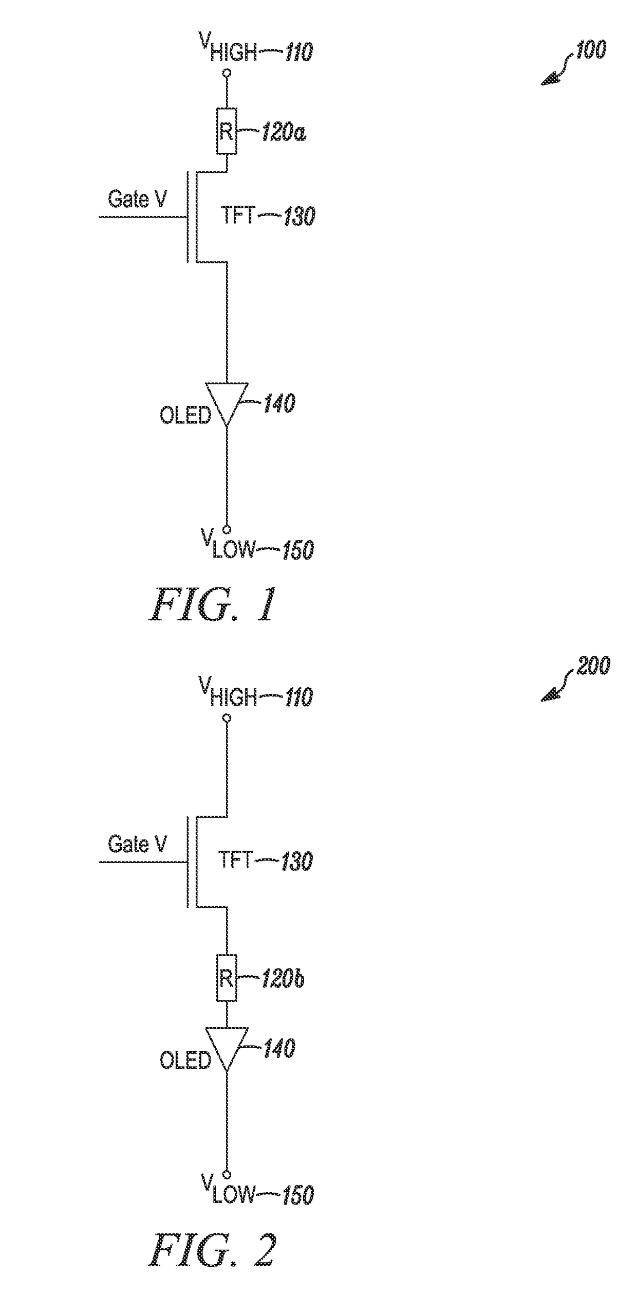
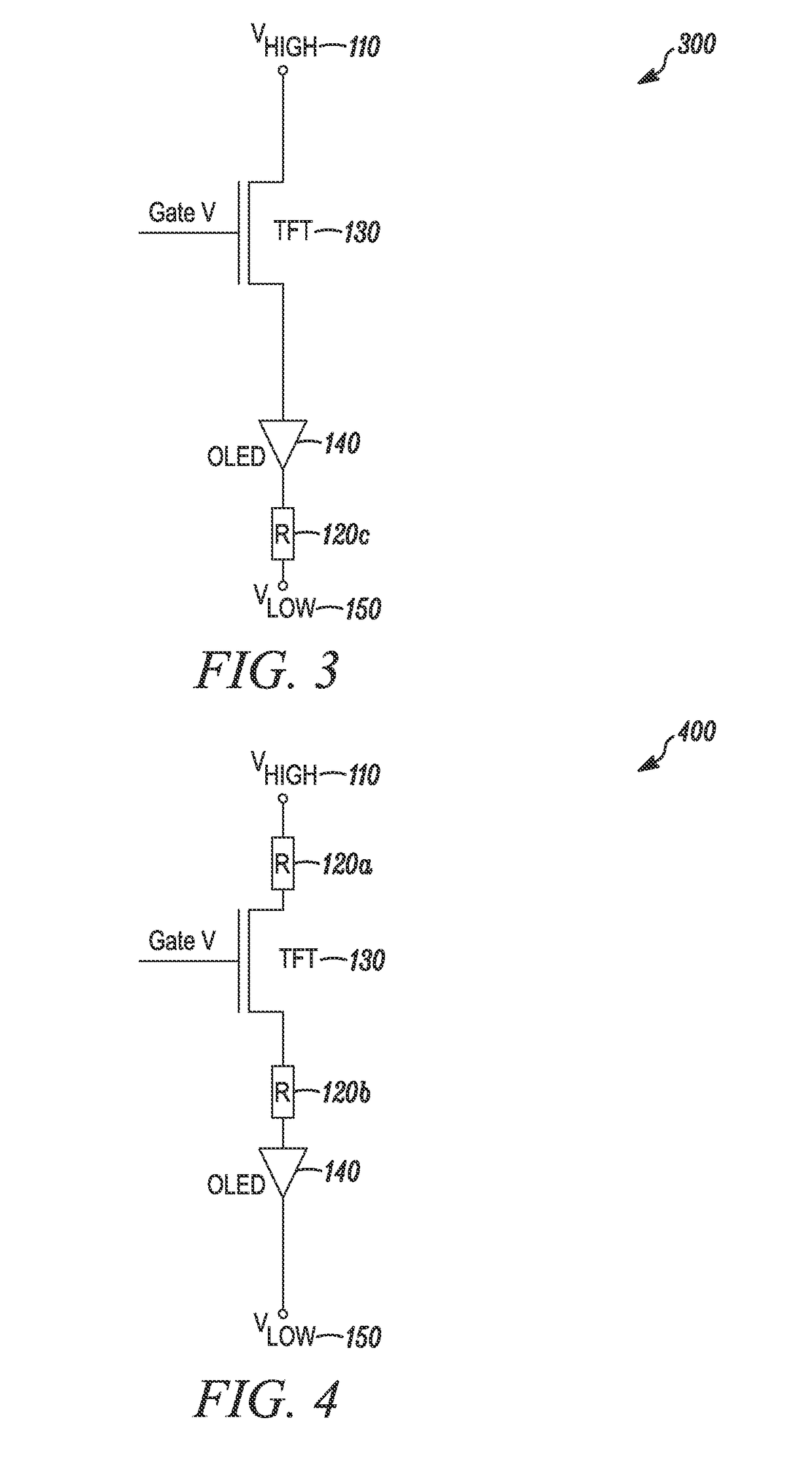
The invention aims to solve issues with printing liquid onto a backplane when creating display devices. Small variations in liquid volume can lead to noticeable differences in display quality, which is sensitive to regular patterns. To address this, the invention introduces a random variation of luminance values, which can raise the quality threshold from 1-2% to 5%. This can be achieved by using different techniques such as altering the conductivity of amorphous or polysilicon material or adding nickel chromium material to the conduction path of the TFT design. The invention provides a more uniform and higher quality display device.

Problems solved by technology

Small variations in the volume of liquid composition deposited can result in small but noticeable variations in the luminance uniformity of the resultant display device.
Within the display industry, regular patterns of 1-2% are discernable to the human eye, and this type of systematic variation lowers the quality threshold for acceptable quality display devices.

Method used


Image

  • Electrical device to mask systematic luminance variation
  • Electrical device to mask systematic luminance variation
  • Electrical device to mask systematic luminance variation

Examples


Embodiment Construction

[0029]Many aspects and embodiments have been described above and are merely exemplary and not limiting. After reading this specification, skilled artisans appreciate that other aspects and embodiments are possible without departing from the scope of the invention.

[0030]Other features and benefits of any one or more of the embodiments will be apparent from the following detailed description, and from the claims.

[0031]Definitions and Clarification of Terms

[0032]Before addressing details of embodiments described below, some terms are defined or clarified.

[0033]The term “active” when referring to a layer or material, is intended to mean a layer or material that exhibits electronic or electro-radiative properties. In an electronic device, an active material electronically facilitates the operation of the device. Examples of active materials include, but are not limited to, materials which conduct, inject, transport, or block a charge, where the charge can be either an electron or a hole,...


PUM


Abstract

An electrical device containing pixel circuits, where at least one resistor is present within one pixel circuit to mask systematic luminance variation in organic light emitting diodes. The resistor can be located at one or more locations between electrodes. Each resistor has a defined resistor density, with distinct resistor values among pixel circuits to produce random variations in pixel luminance across a display containing plurality of pixel circuits.

Description

BACKGROUND OF THE INVENTION[0001]Field of the Invention[0002]This invention relates to an electrical device containing luminescent diodes. In particular, an electrical device having pixel circuits for organic light emitting diodes, the organic light emitting diodes resulting from liquid deposition of organic semiconductor material on a backplane. More particularly, the incorporation of resistors into a multitude of pixel circuits thereby masking systematic luminance variation resulting from off-specification liquid deposition of luminescent materials. The electrical device containing luminescent diodes, also called a display device, can be mounted on the backplane containing a rigid or flexible substrate. The backplane typically contains electrical elements for pixel circuits and may also include thin film transistors for each pixel. Deposition of organic semiconductor materials on these backplanes, including liquid phase deposition, can produce non-uniformities in the resultant lum...

Claims


Application Information

Patent Timeline
Patent Type & Authority Applications(United States)
IPC IPC(8): H01L27/32
CPCH01L27/326H01L27/3262G09G3/3233G09G2320/0233G09G3/32H10K59/1213H10K59/121
Inventor JOHNSON, ANDREW WESLEYTRUJILLO, JOHANN THOMAS
Owner LG CHEM LTD
Learn More