Position sensitive photo detector

a photo detector and position sensitive technology, applied in the direction of measuring devices, instruments, electrical equipment, etc., can solve the problems of limited sensitivity, inability to use in very many applications, and inability to completely guarantee the type, so as to improve the electrical properties of transistors and the effect of changing the conductivity parameters

Inactive Publication Date: 2004-05-13
SITEK ELECTRO OPTICS
View PDF6 Cites 0 Cited by
  • Summary
  • Abstract
  • Description
  • Claims
  • Application Information

AI Technical Summary

Benefits of technology

[0011] Furthermore, it is advantageous to design the collecting electrode as a base in an additional transistor obtained by introduction of additional doped barrier layers. This transistor can be used to further amplify the already amplified and divided, radiation-generated current.
[0012] The barrier layers can be manufactured either by doping the base material of the detector wafer with impurities in such manner that its conductivity parameters (type of conductivity and conductibility) are altered or by using different semiconductor materials having different band gaps in the different conductive layers. The latter way, involving so-called heterojunctions, may improve the electrical properties of the transistor.

Problems solved by technology

A disadvantage of such previously known devices is, however, that the sensitivity, i.e. how much current that is generated by the point of light and that can be divided between the electrodes, is limited by the number of charge carrier pairs that are being generated for each incident radiation quanta.
The consequence of this is that a detector of the above type cannot be used in very many applications or that the result is not entirely reliable.

Method used


Image

  • Position sensitive photo detector
  • Position sensitive photo detector
  • Position sensitive photo detector

Examples


first embodiment

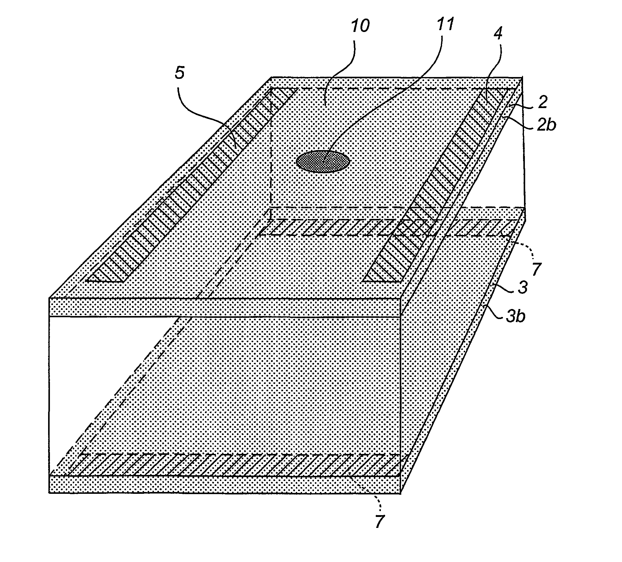
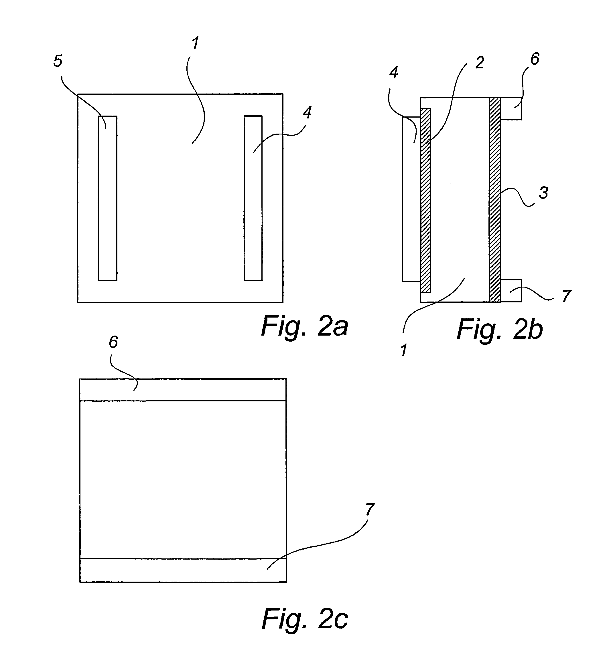
[0022] the device according to the invention, as shown in FIGS. 1 and 2a-c, comprises a semiconductor wafer 1 of a conductivity type n or p with two conductive layers 2 and 3 on either side of the wafer obtained by means of doping. The conductivity type of the doped areas has been selected so as to be the opposite of that of the semiconductor wafer. If, for example, the wafer is of N-type, then the doping of the layer is of P-type. The inverse relation is also possible. In this way, the conductive layers will also constitute barrier layers. Pairs of electrodes 4 & 5 and 6 & 7 respectively are arranged on the conductive layers. The electrodes should be arranged two by two in parallel, and in such manner that each pair extends in a different direction, said direction being preferably perpendicular to that of the other pair. Furthermore, the electrodes are preferably so designed and arranged that each of the two pairs defines two opposite sides of an orthogonal square, which defines tw...

second embodiment

[0028] the device according to the invention, as shown in FIGS. 3 and 4a-c, comprises a semiconductor wafer 1 of a conductivity type n or p with a conductive layer 2 obtained by means of doping and of the opposite conductivity type to that of the base material of the wafer. This conductivity layer also forms, in the same way as described above, a barrier layer. In the same way as described above, a conductive layer 3 is arranged under the barrier layer. In this embodiment, however, the conductivity type of said layer is the same as that of the base material of the wafer. This layer may be formed of the base material of the wafer. In the same way as described above, electrodes 4, 5 and 6, 7 are arranged in contact with the conductive layers. The device according to this embodiment further comprises additional barrier layers 8 and 9, which are required to provide amplification and which are arranged under the electrodes arranged in contact with the conductive layer 3. These barrier la...

third embodiment

[0029] According to the invention, the additional barrier layers 8, 9 may alternatively be arranged under the electrodes arranged in contact with the conductive layer 2, as shown in FIG. 5 and FIGS. 6a-c.

[0030] In the same way as described above, the radiationgenerated current in the two latter embodiments will be amplified and divided, on the basis of which it is possible to determine the location of the irradiated point.


PUM


Abstract

A radiation detector of the type, which by means of electric signals indicates the position of an irradiated point (11) on a detector surface (10) of the detector. The detector comprises a semiconductor wafer (1) comprising at least two barrier layers (2, 3), which are arranged in such manner that when applying an electric bias across the layers, one layer is reversely biased and the other is forwardly biased, the extension of the reversely biased barrier layer substantially coinciding with the detector surface. The detector further comprises at least two conductive layers (2b, 3b, 2, 3) provided with at least one current collecting electrode (4, 5; 6,7), the conductive layers being arranged so as to allow a transistor amplification between the forwardly and reversely biased layer by means of charge currents generated by the radiation in the irradiated point and separated by the reversely biased barrier layer.

Description

[0001] The present invention relates to a radiation sensitive position detector of the type, which by means of electric signals indicates the position of a point located on the active surface of the detector and exposed to electromagnetic radiation. This type of detector is common in measurements where the radiation consists of light, but there are also other applications, where for example the radiation may consist of some form of radioactive or infrared radiation. Therefore, radiation here means any type of electromagnetic radiation. In the following, reference will be made mainly to light, but it will be appreciated that the discussion also generally applies to all electromagnetic radiation.[0002] A detector of the above type is built on a semiconductor wafer of the type in which a concentrated radiation causes charge carrier pairs (holes and electrons) to form in the irradiated point.[0003] The semiconductor wafer is provided with conductive layers, one of which also serves as a...

Claims


Application Information

Patent Timeline
Patent Type & Authority Applications(United States)
IPC IPC(8): G01B11/03H01L31/16H01LH01L31/00H01L31/02H01L31/0328H01L31/10H01L31/11
CPCH01L31/1105H01L31/02024
Inventor LINDHOLM, LARS
Owner SITEK ELECTRO OPTICS
Why Eureka
Try Eureka