Structure for Memory Chip for High Capacity Memory Subsystem Supporting Replication of Command Data

a memory chip and command data technology, applied in the direction of electric digital data processing, instruments, computing, etc., can solve the problems of path consumption a larger share of access time, memory subsystem and speed at which it operates, inability to perform useful work, etc., to reduce the number of i/o ports, reduce the frequency of bus operations, and save power

Active Publication Date: 2009-01-01
LENOVO GLOBAL TECH INT LTD
View PDF26 Cites 19 Cited by
  • Summary
  • Abstract
  • Description
  • Claims
  • Application Information

AI Technical Summary

Benefits of technology

[0022]By configuring memory chips which can be used for daisy chaining in an interleaved tree configuration according to the preferred embodiment, a larger volume of memory can be configured to a limited number of buses supported by the memory controller without using custom memory chips. Additionally, the interleaved configuration has the potential to achieve significant power savings by both reducing the frequency of bus operations of many (although not necessarily all) of the buses, and by reducing the number of I / O ports which are actually used.

Problems solved by technology

In operation, the processor is constantly accessing instructions and other data in memory, without which it is unable to perform useful work.
The design of the memory subsystem and speed at which it operates are critical issues in the overall performance of any computer system.
As computers have grown more complex, this path has consumed a larger share of the access time.
In these systems, it is simply not possible for direct paths to exist from every processor to every memory module.
If design of future standardized memory modules is optimized for low-end systems, these modules may be inefficient when used in larger systems having different design parameters.
It would be possible to design a separate set of memory modules for use in larger systems, but this would lose the economies of scale available in using high-volume, standardized memory modules, and substantially increase the cost of larger systems.

Method used


Image

  • Structure for Memory Chip for High Capacity Memory Subsystem Supporting Replication of Command Data
  • Structure for Memory Chip for High Capacity Memory Subsystem Supporting Replication of Command Data
  • Structure for Memory Chip for High Capacity Memory Subsystem Supporting Replication of Command Data

Examples


Embodiment Construction

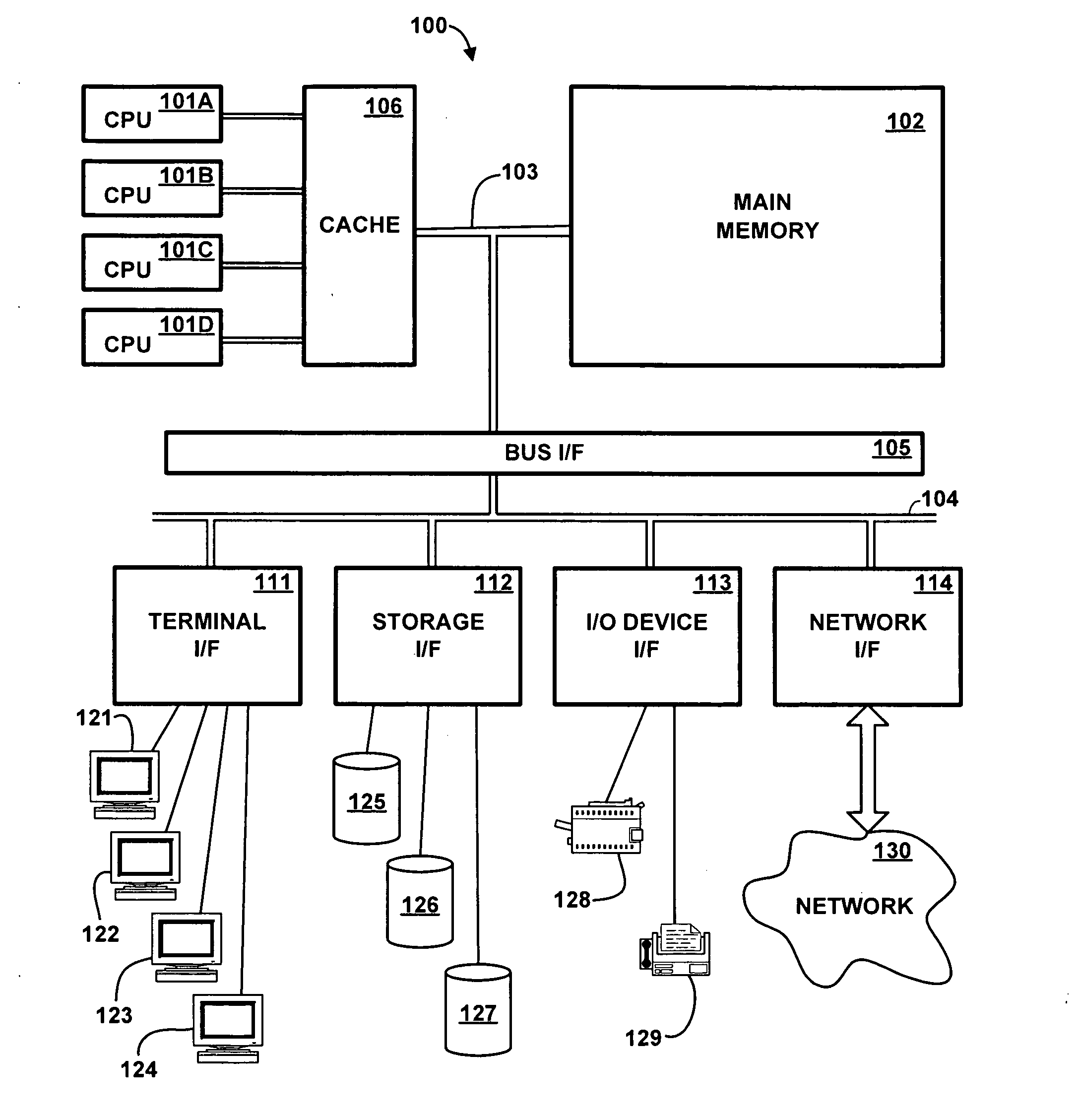
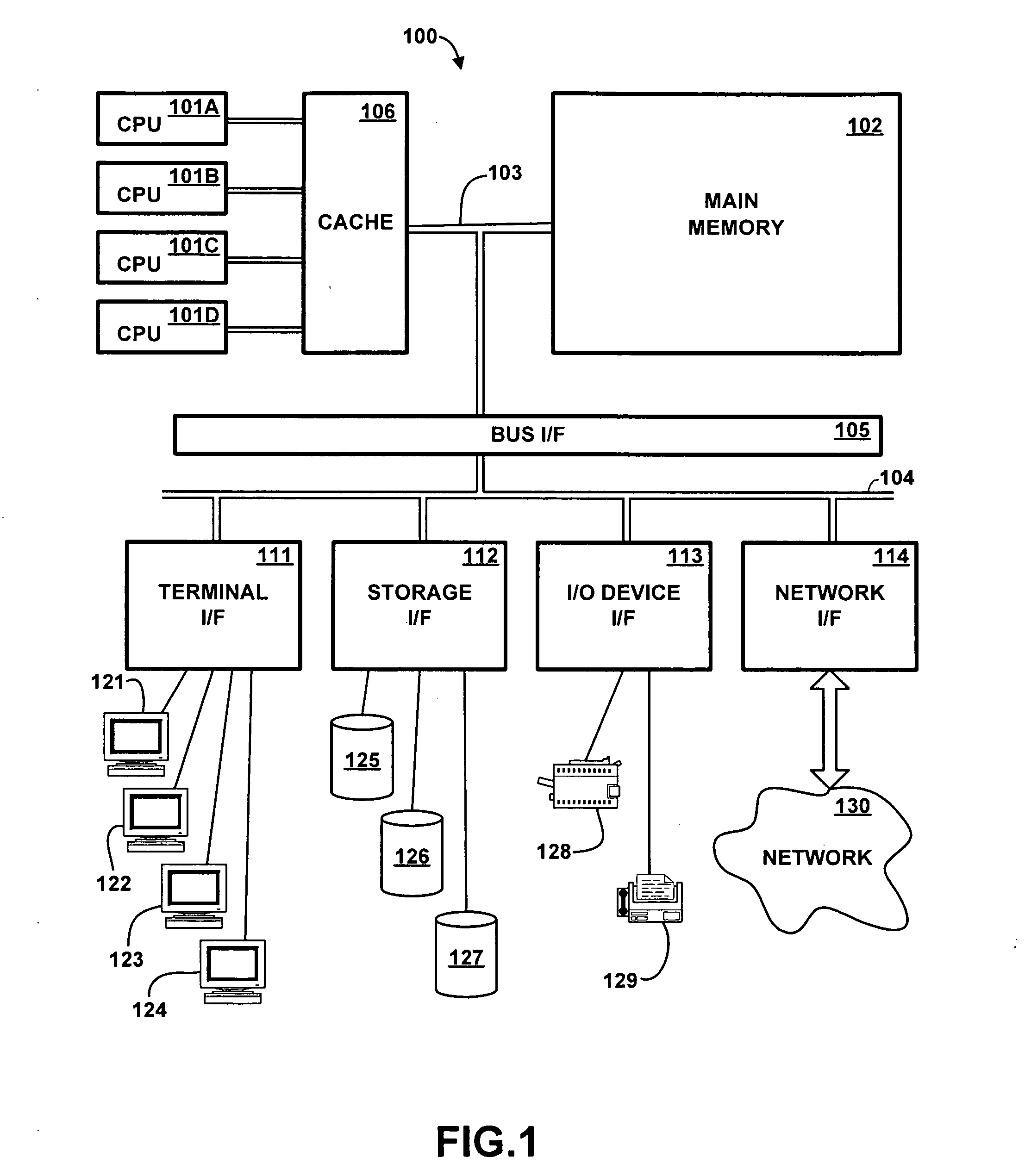
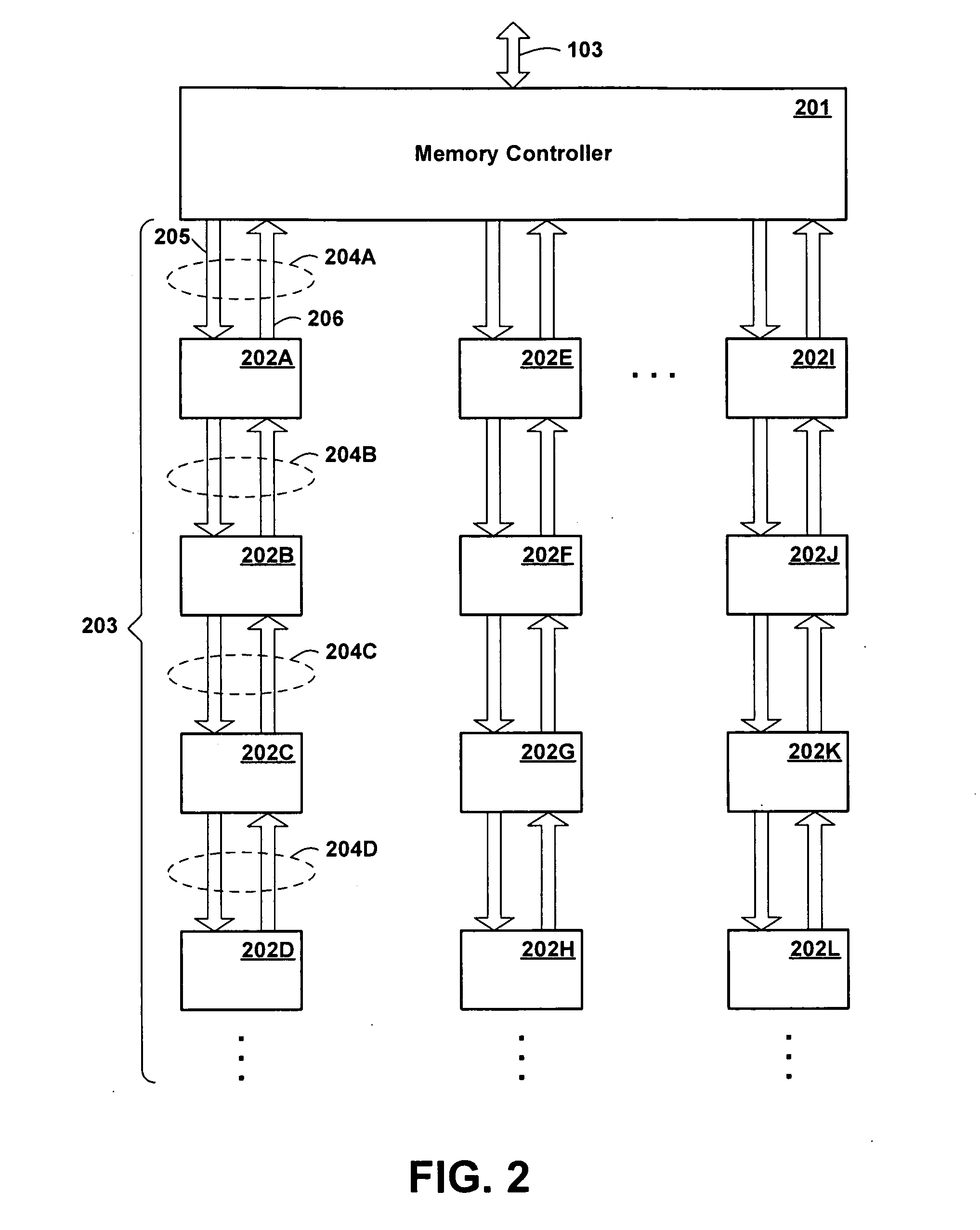
Future Memory Chip Overview

[0032]Low-end systems typically require large memory bandwidth, i.e. the ability to read and write a large amount of memory in a given time, but do not necessarily require large memory capacities. In order to meet these requirements, the present inventors envision a buffered memory chip and memory chip architecture supporting chains of memory chips. Such an architecture is described in the following commonly assigned copending patent applications, each of which is herein incorporated by reference: U.S. application Ser. No. 11 / 459,956, filed Jul. 26, 2006, entitled “Daisy Chained Memory System”; U.S. application Ser. No. 11 / 459,957, filed Jul. 26, 2006, entitled “Memory System Having Self Timed Daisy Chained Memory Chips”; U.S. application Ser. No. 11 / 459,969, filed Jul. 26, 2006, entitled “Carrier Having Daisy Chained Memory Chips”; U.S. application Ser. No. 11 / 459,983, filed Jul. 26, 2006, entitled “Carrier Having Daisy Chain of Self Timed Memory Chips”; ...


PUM


Abstract

A design structure is provided for a memory module containing a first interface for receiving data access commands and a second interface for re-transmitting data access commands to other memory modules, the second interface propagating multiple copies of received data access commands to multiple other memory modules. The memory module is preferably used in a high-capacity memory subsystem organized in a tree configuration in which data accesses are interleaved. Preferably, the memory module has multiple-mode operation, one of which supports multiple replication of commands and another of which supports conventional daisy-chaining

Description

CROSS REFERENCE TO RELATED APPLICATIONS[0001]This is a continuation-in-part of U.S. patent application Ser. No. 11 / 769,001, filed Jun. 27, 2007, entitled “Memory Chip for High Capacity Memory Subsystem Supporting Replication of Command Data”, which is herein incorporated by reference. This application claims priority under 35 U.S.C. §120 of U.S. patent application Ser. No. 11 / 769,001, filed Jun. 27, 2007.[0002]The present application is related to the following commonly assigned copending U.S. patent applications, filed on the same date as the present application, all of which are herein incorporated by reference:[0003]U.S. patent application Ser. No. 11 / 768,988, filed Jun. 27, 2007, entitled “High Capacity Memory Subsystem Architecture Employing Hierarchical Tree Configuration of Memory Modules”;[0004]U.S. patent application Ser. No. 11 / 768,995, filed Jun. 27, 2007, entitled “High Capacity Memory Subsystem Architecture Storing Interleaved Data for Reduced Bus Speed”;[0005]U.S. pate...

Claims


Application Information

Patent Timeline
Patent Type & Authority Applications(United States)
IPC IPC(8): G06F12/00
CPCG06F13/1684G06F12/084
Inventor BARTLEY, GERALD K.BORKENHAGEN, JOHN M.GERMANN, PHILIP RAYMOND
Owner LENOVO GLOBAL TECH INT LTD
Why Eureka
Try Eureka