Display device and electronic device using the same

a technology of electronic devices and display devices, applied in the field of display devices of digital gray scale methods and electronic devices using the same, can solve the problems of deterioration of light emitting elements such as el elements by long time of light emission, increasing the amount of video data according, and reducing the number of writing to nonvolatile memory. , to achieve the effect of low power consumption, low access speed, and low cos

Active Publication Date: 2009-01-15
SEMICON ENERGY LAB CO LTD
View PDF26 Cites 9 Cited by
  • Summary
  • Abstract
  • Description
  • Claims
  • Application Information

AI Technical Summary

Benefits of technology

[0041]In each frame period, only correction video data corresponding to one of the first to n-th pixel regions is transmitted from the arithmetic circuit to the adder of the counter portion while accumulated light emission time of a pixel in the selected pixel region is read our from the memory circuit portion and transmitted to the adder, and then the accumulated light emission time and the correction video data are added so that the accumulated light emission time is updated, thereby the number of reading out the accumulated light emission time from the memory circuit portion to the adder can be reduced and an inexpensive memory with low power consumption and low access speed can be used as the memory circuit portion.
[0042]As another method, in each frame period, the deterioration compensation circuit may output to the panel controller correction video data corresponding to one of the first to n-th pixel regions and non-correction video data corresponding to the other pixel regions. Such a deterioration compensation circuit further includes a selector provided between the arithmetic circuit and the correction data storing portion. The selector includes two input terminals and one output terminal. The output terminal is connected to an input terminal of the correction circuit, and one of the two input terminals is connected to the output terminal of the correction data storing portion. A predetermined value is inputted to the other of the two input terminals. The selector operates so that the correction data stored in the correction data storing portion is inputted to the arithmetic circuit when video data corresponding to one of the first to n-th pixel regions is inputted to the arithmetic circuit, and so that a predetermined value is inputted to the arithmetic circuit when video data corresponding to the other pixel regions is inputted to the arithmetic circuit. The predetermined value may be a value which does not change video data even when the arithmetic circuit applies an arithmetic operation to the video data. With such a structure, video data corrected in the arithmetic circuit is also 1 / n of the inputted video data. Further, the number of pixels of which accumulated light emission time is actually updated at a regular update of the accumulated light emission time becomes 1 / n of the total number of pixels. Accordingly, the number of reading of the accumulated light emission time of a pixel stored in the memory circuit portion is reduced to 1 / n for generating an address for reading out correction data used for video data correction from the correction data storing portion is reduced to 1 / n, therefore, an inexpensive memory with low power consumption and low access speed can be used as the memory circuit portion.
[0043]In each frame period, in the case where the correction video data corresponding to one of the first to n-th pixel regions and the non-correction video data corresponding to the other pixel regions are transmitted from the arithmetic circuit to the counter portion, the counter portion includes an adder and a latch connected to an input terminal of the adder. The latch of the counter portion regularly samples only the correction video data corresponding to the one of the first to n-th pixel regions and transmits the data to the adder. The adder reads out from the memory circuit portion the accumulated light emission time of a pixel in the pixel region in which the correction video data is transmitted to the adder, so that the accumulated light emission time is updated by adding the correction video data to the accumulated light emission time. Accordingly, the number of reading out the accumulated light emission time from the memory circuit portion to the adder can be reduced, thereby an inexpensive memory with low power consumption and low access speed can be used as the memory circuit portion.
[0044]The aforementioned display device is preferably a display device of a time gray scale method. By using the aforementioned display device to form an electronic device, cost reduction and downsizing of the electronic device can be easily realized.

Problems solved by technology

In recent years, however, the amount of video data tends to increase according to the increasing size of the display panel, and there is a case where video data of one frame is not stored in one SRAM.
On the other hand, a light emitting element such as an EL element is deteriorated by long time of light emission.
However, the number of writing to the nonvolatile memory is generally limited, therefore, data is written to the volatile memory 13 in operation of the display device 17 while the data is written to the nonvolatile memory 14 at a certain interval (for example, per hour, at shutdown of a power source, or the like).
Accordingly, a component (especially a memory) capable of fast speed operation is required, which leads to increase the cost.

Method used


Image

  • Display device and electronic device using the same
  • Display device and electronic device using the same
  • Display device and electronic device using the same

Examples


Embodiment Construction

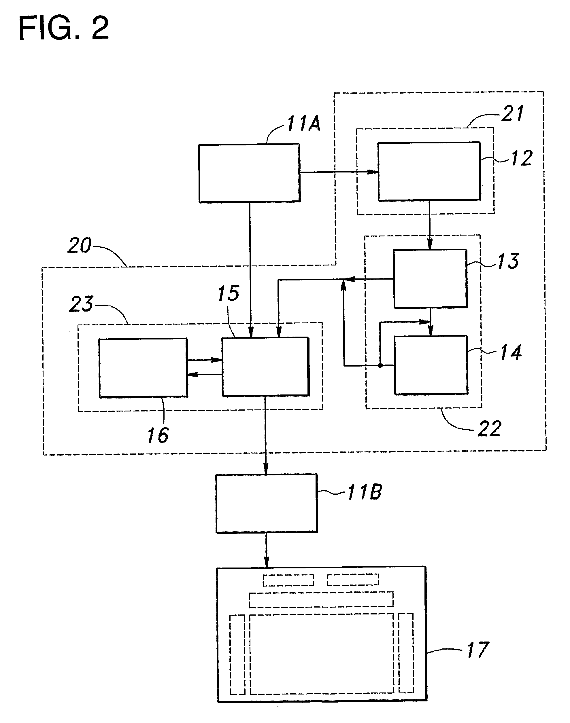
[0056]Hereinafter described with reference to the drawings is an embodiment mode of the invention.

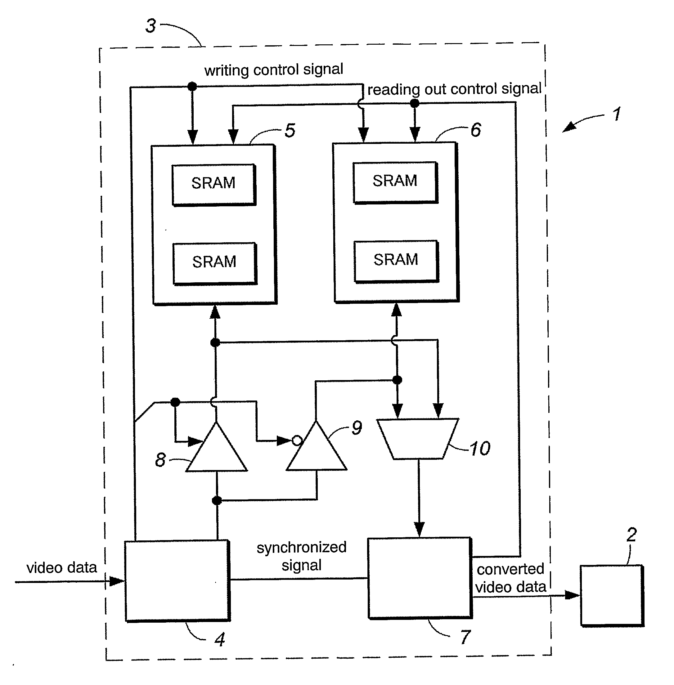
[0057]FIG. 3 is a block diagram showing a preferred embodiment of a display device according to the invention. A display device 31 includes an active matrix display panel 32 using a self-luminous material such as an organic EL material and a panel controller 33 which converts the format of inputted video data and supplies the converted video data to the display panel 32 at an appropriate timing.

[0058]The panel controller 33 includes a format converter portion 34, a first video memory 35, a second video memory 36, a display control portion 37, a first tri-state buffer 38, a second tri-state buffer 39, and a selector 40 similarly to the conventional example shown in FIG. 1.

[0059]In this embodiment shown in FIG. 3, pixels of the display panel 32 are divided into, for example, first and second pixel regions. The format converter portion 34 converts the format of only video data correspondin...


PUM


Abstract

According to the invention, a compact and inexpensive with low power consumption memory and low access speed can be used for a panel controller and a deterioration compensation circuit of a display device. In a display device of a digital gray scale method, a plurality of pixels of a display panel are divided into first to n-th pixel regions (n is 2 or more) and a format converter portion of a panel controller converts the format of only video data corresponding to one of first to n-th pixel regions and writes the data to one of first and second video memories in each frame period. A display control portion reads out video data that is converted in format and corresponds to one of first to n-th pixel regions in which video data is written to the other of the first and second video memories in the preceding frame period, and transmits the data to the display panel.

Description

TECHNICAL FIELD[0001]The present invention relates to a display device of a digital gray scale method and an electronic device using the same. In particular, the invention relates to a display device of a time gray scale method using a self-luminous material such as an organic electroluminescence (EL) and to an electronic device using the same.BACKGROUND ART[0002]In recent years, an active matrix semiconductor display device is attracting attentions in the market as a flat panel display (FPD). In particular, a self-luminous type active matrix display device using a self-luminous material such as an organic EL is attracting attentions and actively researched and developed as a flat panel display substituting a liquid crystal display (LCD).[0003]An active matrix display device is known to be operated by an analog gray scale method in which luminance of each pixel is continuously changed or a digital gray scale method in which luminance of each pixel is pervasively changed. The analog ...

Claims


Application Information

Patent Timeline
Patent Type & Authority Applications(United States)
IPC IPC(8): G09G5/02G09G3/30G09G3/22
CPCG09G3/2022G09G3/3225G09G5/399G09G2320/048G09G2320/0247G09G2320/0285G09G2310/0227G09G3/20G09G3/30G09G3/36G09G5/36
Inventor OZAKI, TADAFUMIENDO, MASAMI
Owner SEMICON ENERGY LAB CO LTD
Why Eureka
Try Eureka