IC device and method of manufacturing the same
- Summary
- Abstract
- Description
- Claims
- Application Information
AI Technical Summary
Benefits of technology
Problems solved by technology
Method used
Image
Examples
first embodiment
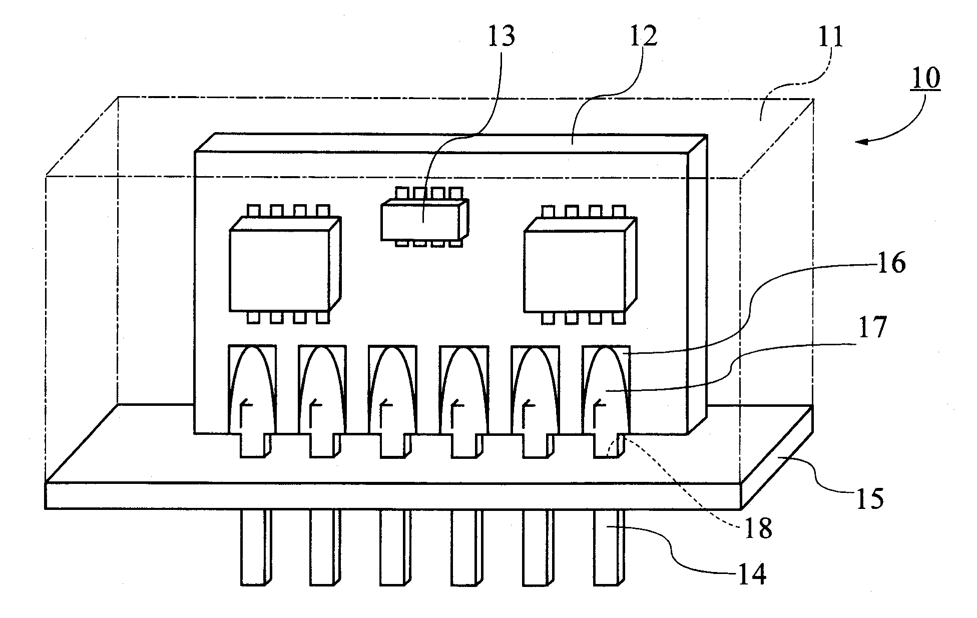
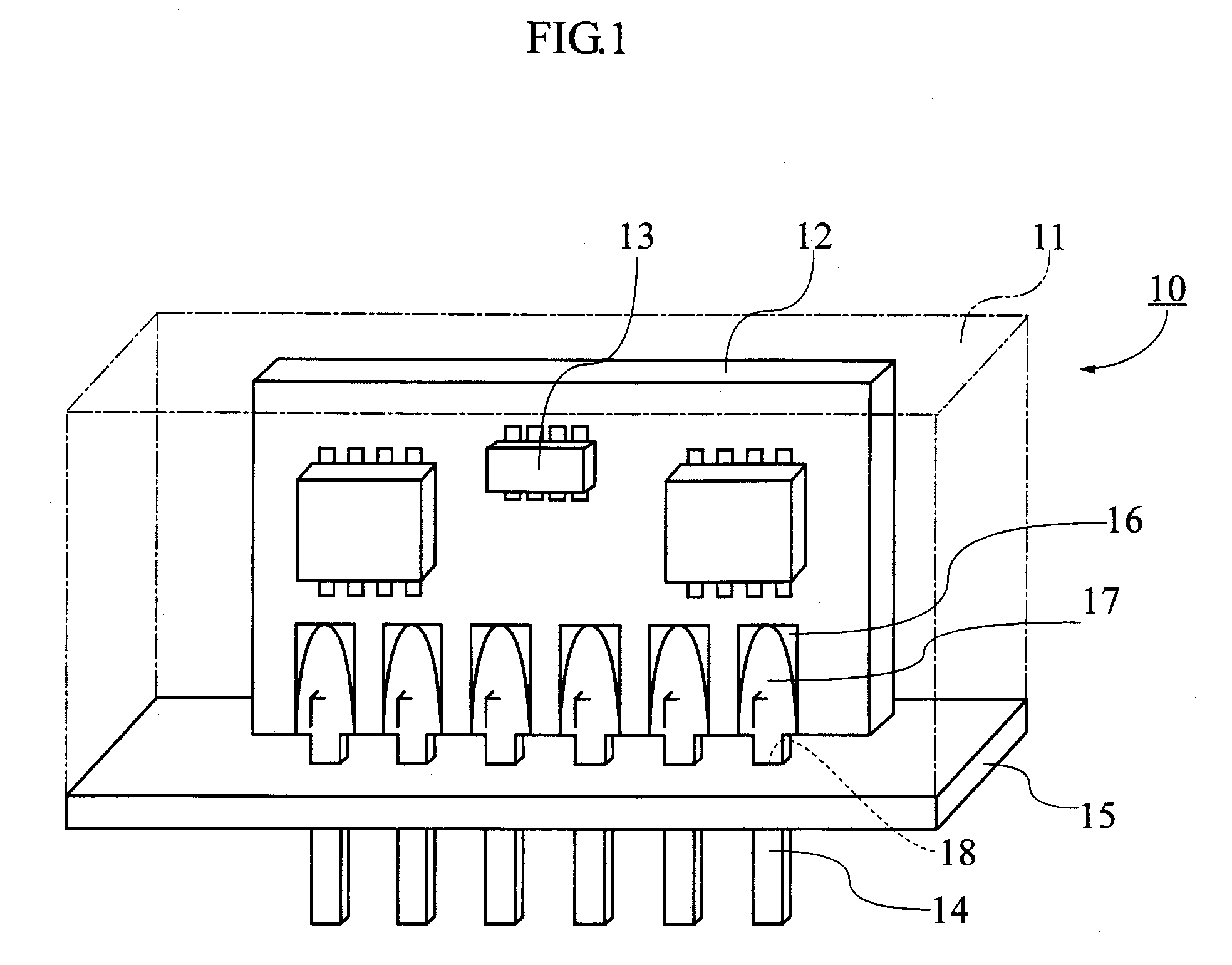
[0029]FIGS. 1 to 4 illustrate the present invention. As shown in FIG. 1, an IC device 10 of the present invention includes a resin package 11, a printed circuit board 12, a functional component 13, and a plurality of terminal pins 14. The resin package 11 encloses the circuit board 12 and the functional component 13 mounted on the circuit board 12. The circuit board 12 is provided with a wiring pattern (not shown) and a plurality of pads 16 connected to the wiring pattern. The terminal pins 14 are connected to the pads 16, respectively, via solder 17. The functional component 13 is connected to selected ones of the pads 16 (and hence the terminal pins 14) via the unillustrated wiring pattern. The functional component 13 is, for example, an IC chip, a resistance, a diode, and so forth.
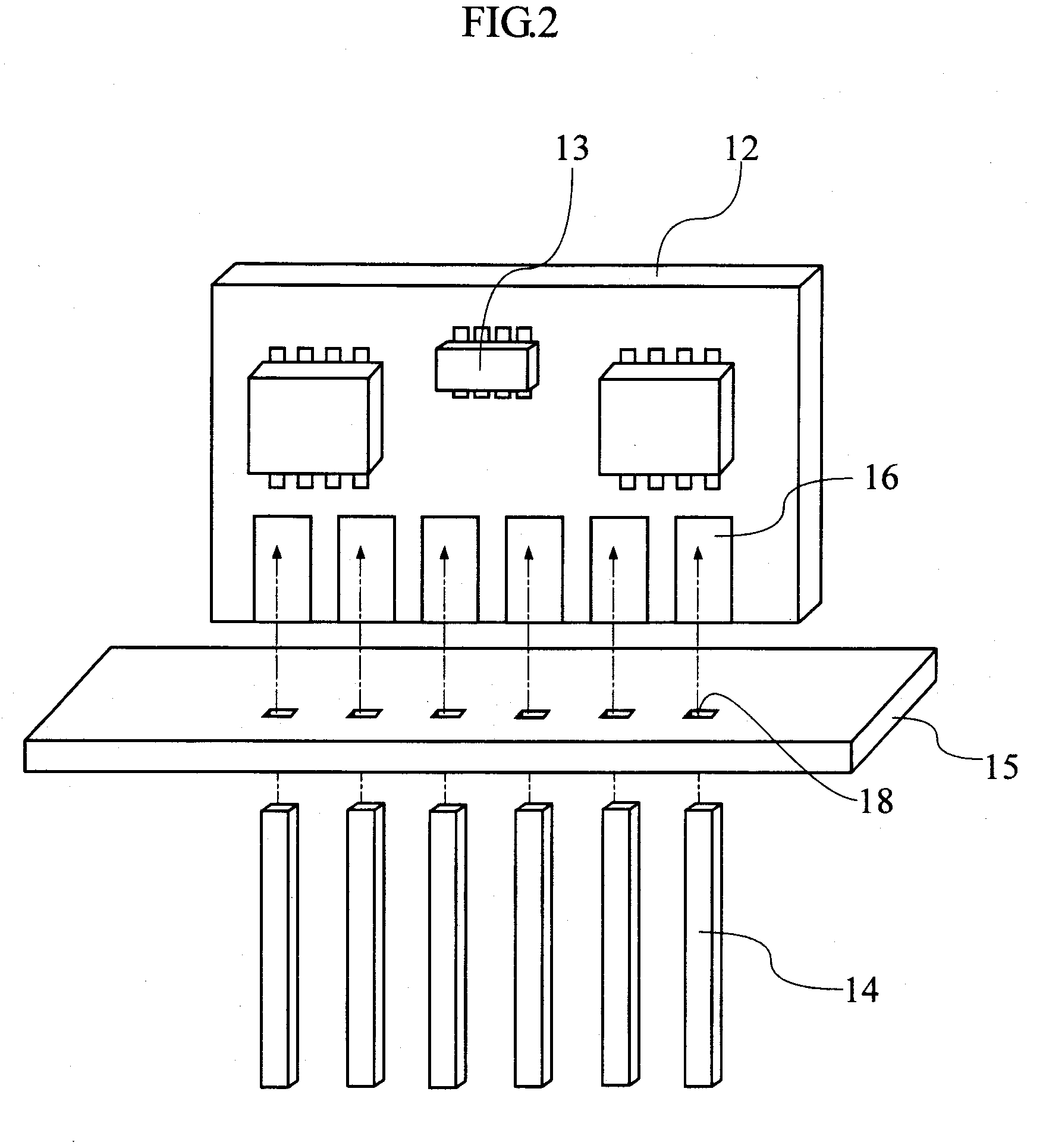
[0030]The IC device 10 also includes a base plate 15 made of an insulating material such as glass epoxy resin. The base plate 15 has upper and lower surfaces both of which are flat and rectangular. The ...
second embodiment
[0038]FIG. 7 depicts a second stage of the manufacturing process. The two molds 19A, 19B employed to form the resin package 11 are brought into contact with the base plate 15. In the second embodiment again, the molds 19A, 19B are of a simple shape, and can be used for making IC devices having different layouts of the terminal pins 14.
[0039]FIGS. 8 to 10 illustrate a third embodiment of the present invention. As seen from FIG. 8, an IC device 30 of this embodiment is different from those of the foregoing-embodiments in that the circuit board 12 is oriented in parallel to the base plate 15. The constituents of the third embodiment that are identical or similar to those of the foregoing embodiments are designated by the same reference numeral, and the description thereof will be omitted.
[0040]FIG. 9 depicts a first stage of the manufacturing process of the IC device 30. The terminal pins 14 each include a flange 31. The flange 31 serves to support the circuit board 12 from below. The ...
PUM
 Abstract
Description
Claims
Application Information


