Process method to fabricate CMOS circuits with dual stress contact etch-stop liner layers
a technology of etching stop and cmos, which is applied in the direction of semiconductor devices, electrical equipment, basic electric elements, etc., can solve the problems of strain loss in the cmos channel region, partial or full delamination of the layers, and the etching process of the second stress layer often thins the underlying first stress layer
- Summary
- Abstract
- Description
- Claims
- Application Information
AI Technical Summary
Problems solved by technology
Method used
Image


Examples
Embodiment Construction
[0001]1. Field of the Invention
[0002]This invention relates generally to complementary metal oxide semiconductor (CMOS) devices and methods for their manufacture and, more particularly, to dual stress layers of CMOS devices.
[0003]2. Background of the Invention
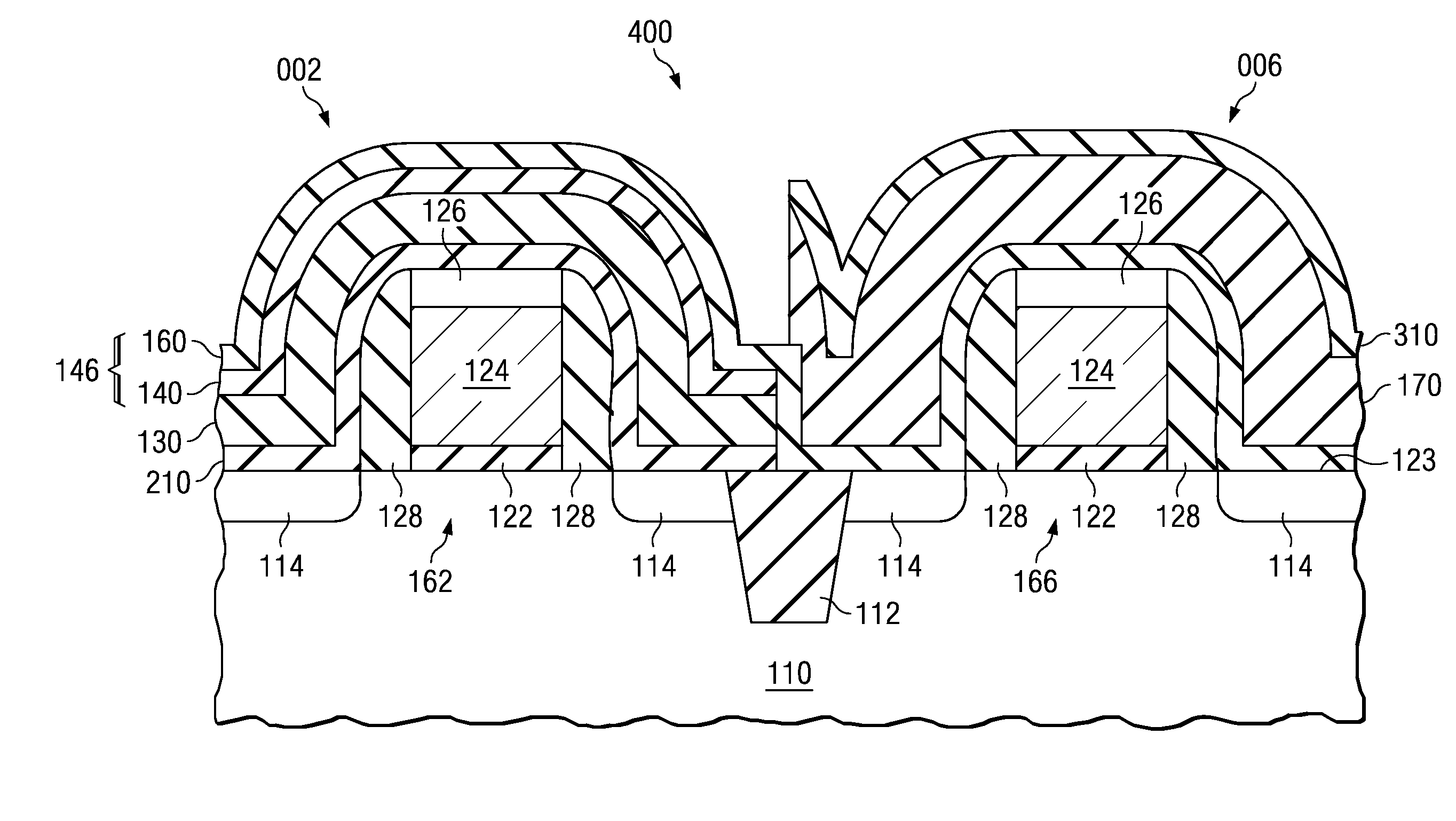
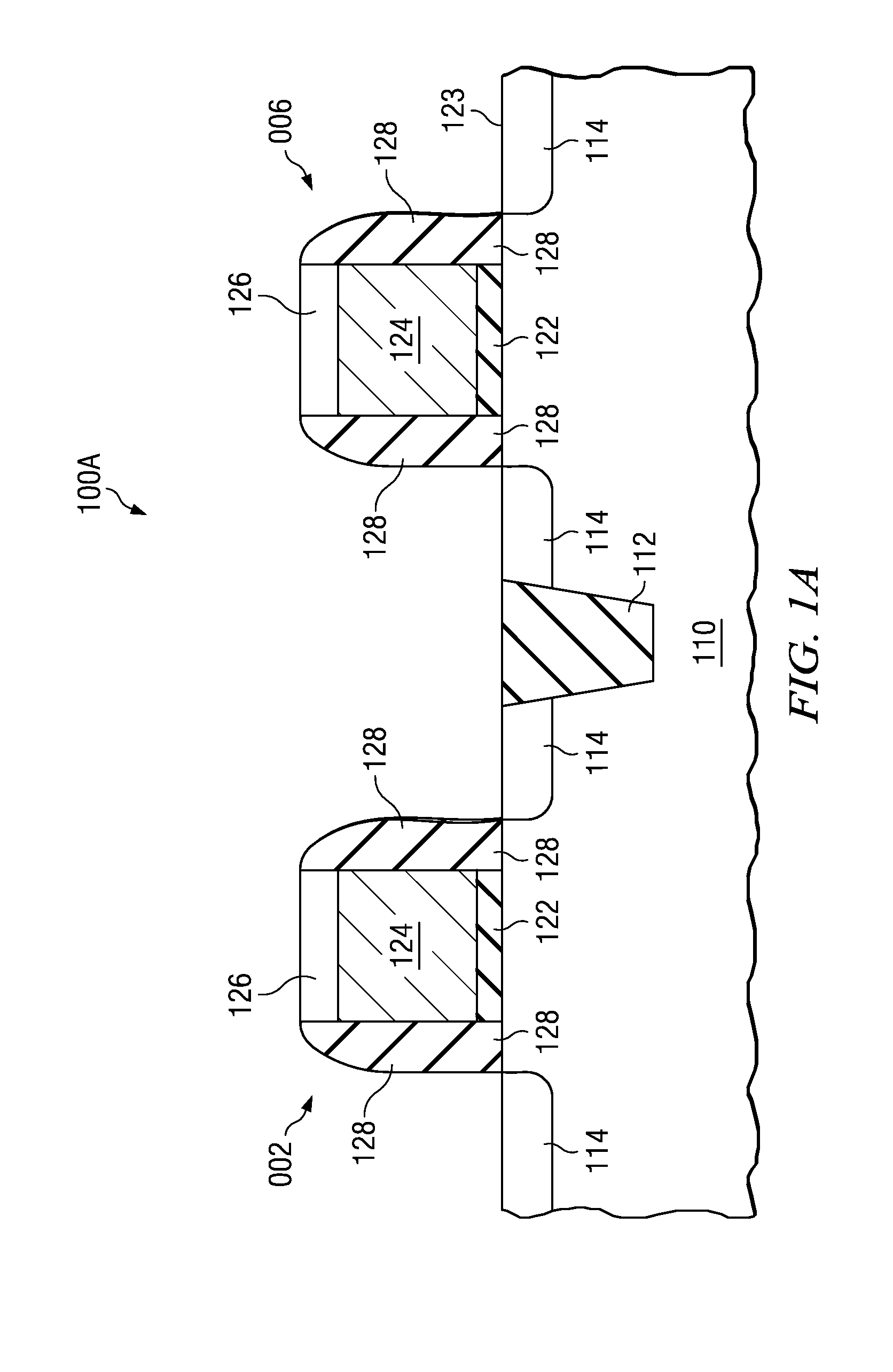
[0004]Dual stress layers (DSL) have been proven to be an effective way to improve both NMOS and PMOS transistor performance of CMOS devices. This is because the carrier mobility of each channel region of the NMOS and PMOS transistors can be increased by the stress exerted in the channel region from its corresponding stress layer.
[0005]Generally, two types of stress layers, including tensile stress layers and compressive stress layers, can be formed over CMOS transistor structures. In a CMOS fabrication process, each stress layer can be deposited, patterned and etched. Often there is a buffer layer formed between the two types stress layers during the fabrication. For example, a second stress layer (e.g., a compressive stress la...
PUM
 Abstract
Description
Claims
Application Information
 - R&D
- Intellectual Property
- Life Sciences
- Materials
- Tech Scout
- Unparalleled Data Quality
- Higher Quality Content
- 60% Fewer Hallucinations
Browse by: Latest US Patents, China's latest patents, Technical Efficacy Thesaurus, Application Domain, Technology Topic, Popular Technical Reports.
© 2025 PatSnap. All rights reserved.Legal|Privacy policy|Modern Slavery Act Transparency Statement|Sitemap|About US| Contact US: help@patsnap.com