
System and Method for Measuring Interferences

a technology of interference measurement and interference, applied in the field of system and method for measuring interference, can solve the problems of high cost of scanning electron microscope, inconvenient use, and inability to accurately measure the interference,

Inactive Publication Date: 2009-02-05
CHUNG YUAN CHRISTIAN UNIVERSITY
View PDF6 Cites 14 Cited by
  • Summary
  • Abstract
  • Description
  • Claims
  • Application Information

AI Technical Summary

Problems solved by technology

SEM (Scanning electron microscope) is expensive to buy and maintain.
While an electron microscope needs an expensive vacuum environment for proper operation, most AFM modes can work perfectly well in ambient air or even a liquid environment.
Nevertheless, a disadvantage of AFM compared with the scanning electron microscope (SEM) is the image size.
Another inconvenience is that at high resolution, the quality of an image is limited by the radius of curvature of the probe tip, and an incorrect choice of tip for the required resolution can lead to image artifacts.
The relatively slow rate of scanning during AFM imaging often leads to thermal drift in the image (Lapshin, 2004, 2007), making the AFM microscope less suited for measuring accurate distances between artifacts on the image.

Method used


Image

  • System and Method for Measuring Interferences
  • System and Method for Measuring Interferences
  • System and Method for Measuring Interferences

Examples


Embodiment Construction

[0017]The present disclosure can be described by the embodiments given below. It is understood, however, that the embodiments below are not necessarily limitations to the present disclosure, but are used to a typical implementation of the invention.

[0018]Having summarized various aspects of the present invention, reference will now be made in detail to the description of the invention as illustrated in the drawings. While the invention will be described in connection with these drawings, there is no intent to limit it to the embodiment or embodiments disclosed therein. On the contrary the intent is to cover all alternatives, modifications and equivalents included within the spirit and scope of the invention as defined by the appended claims.

[0019]It is noted that the drawings presents herein have been provided to illustrate certain features and aspects of embodiments of the invention. It will be appreciated from the description provided herein that a variety of alternative embodimen...


PUM

PropertyMeasurementUnit
heightaaaaaaaaaa
lengthaaaaaaaaaa
refractive indexaaaaaaaaaa

Abstract

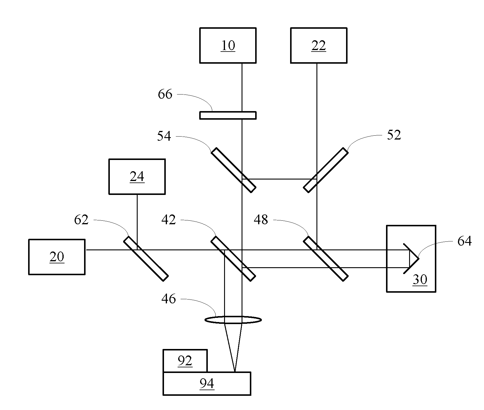
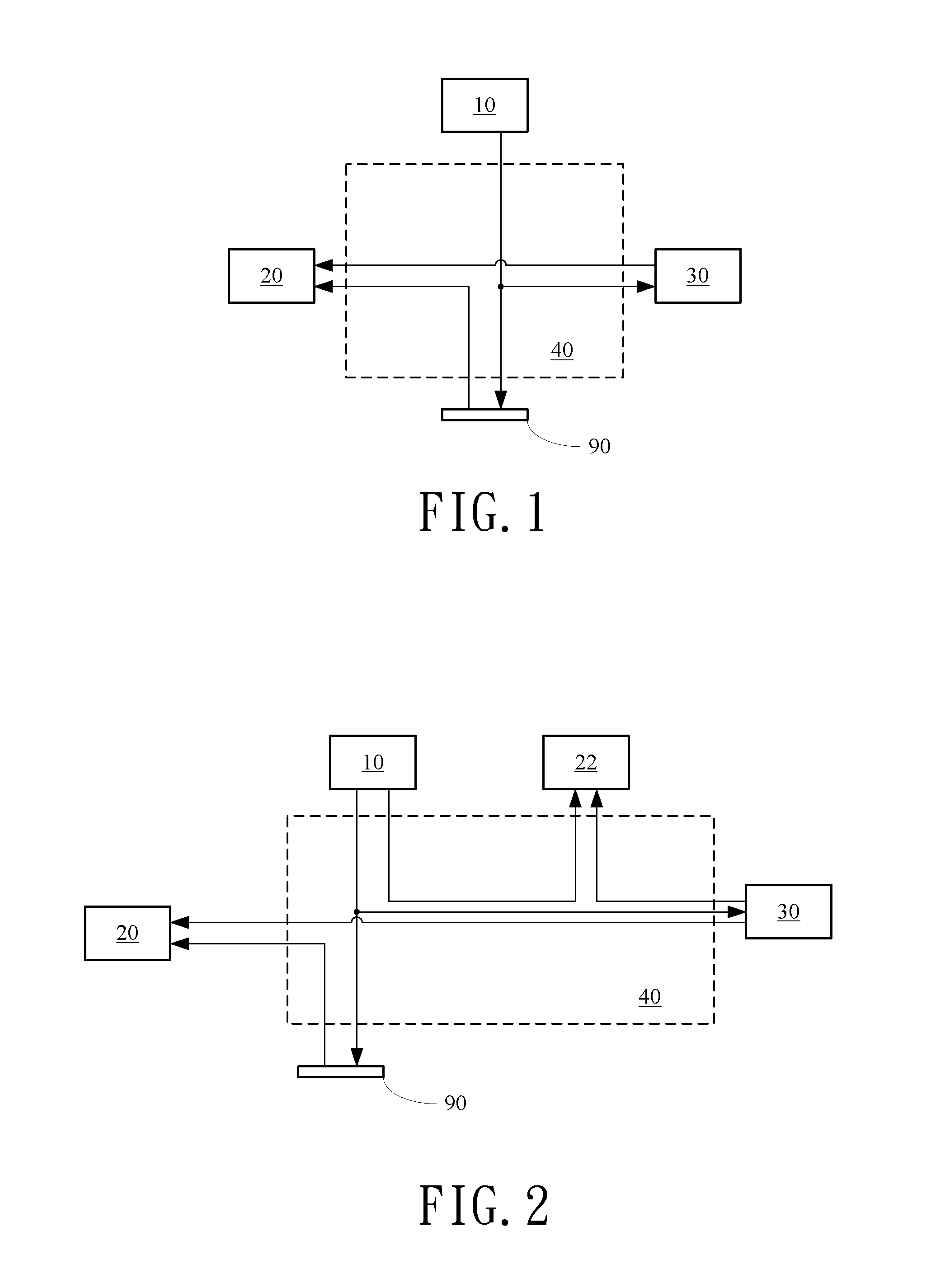
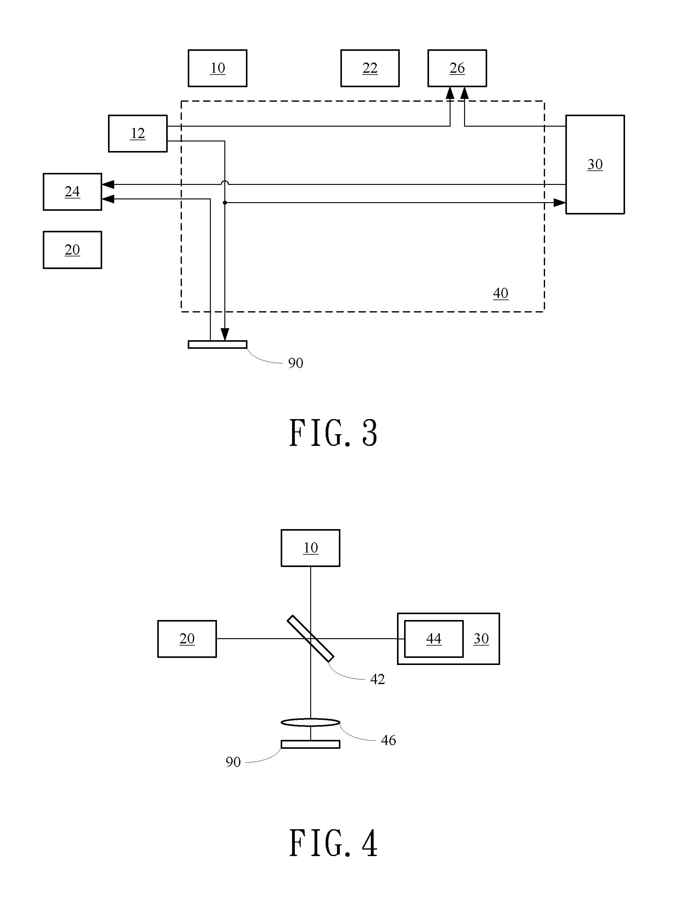
A system and method for measuring interferences are disclosed. The system is based on the concept of a composite interferometer. The sample is measured while a simultaneous compensation of the phase deviation due to the relative displacement of the optical delay component between the measurements at different pixels of the sample is performed. In the application of profilometry, the information of the surface profile of a material is obtained from the phase shift of the interference signal. By using the proposed compensation mechanism, an axial resolution at nanometer scale can be achieved. For the measurement of a thin film, a polarized probe beam is oblique incident on the sample. The system can perform a simultaneous measurement of the refractive index and the thickness of the thin film. From the ratio of the intensities of the interferograms of TE and TM waves as well as the phase shifts of the interferograms, the refractive index and the thickness of the thin film can then be obtained simultaneously.

Description

BACKGROUND OF THE INVENTION[0001]1. Field of the Invention[0002]The present invention generally relates to system and method for measuring interferences.[0003]2. Description of the Prior Art[0004]SEM (Scanning electron microscope) is expensive to buy and maintain. It is dynamic rather than static in its operation: requiring extremely stable high-voltage supplies, extremely stable currents to each electromagnetic coil / lens, continuously-pumped high- / ultra-high-vacuum systems, and a cooling water supply circulation through the lenses and pumps. As it is very sensitive to vibration and external magnetic fields, microscopes aimed at achieving high resolutions must be housed in buildings (sometimes underground) with special services.[0005]However, the AFM (Atomic Force Microscope) has several advantages over the scanning electron microscope (SEM). Unlike the electron microscope which provides a two-dimensional projection or a two-dimensional image of a sample, the AFM provides a true thr...

Claims


Application Information

Patent Timeline
Patent Type & Authority Applications(United States)
IPC IPC(8): G01N21/00G01B11/02
CPCG01B9/02007G01B9/02027G01B2290/45G01B2290/40G01B2290/70
Inventor HSU, I-JENLAI, CHENG-CHUNG
Owner CHUNG YUAN CHRISTIAN UNIVERSITY
Learn More