[0010]At least one of the above and other features and advantages of the present invention may be realized by providing a method of forming a metal wiring for a semiconductor device, including forming a metal-based layer on a substrate, the substrate including at least one conductive structure, forming a metal seed layer on the metal-based layer, forming a supplementary contact layer on the metal seed layer along peripheral portions of the substrate, the supplementary contact layer including a supplementary metal having an electrical resistance smaller than or equal to an electrical resistance of the metal seed layer, loading the substrate into a plating apparatus, such that the supplementary contact may be in direct contact with a cathode of the plating apparatus, and forming the metal wiring layer on the metal-based layer by an electroplating process.
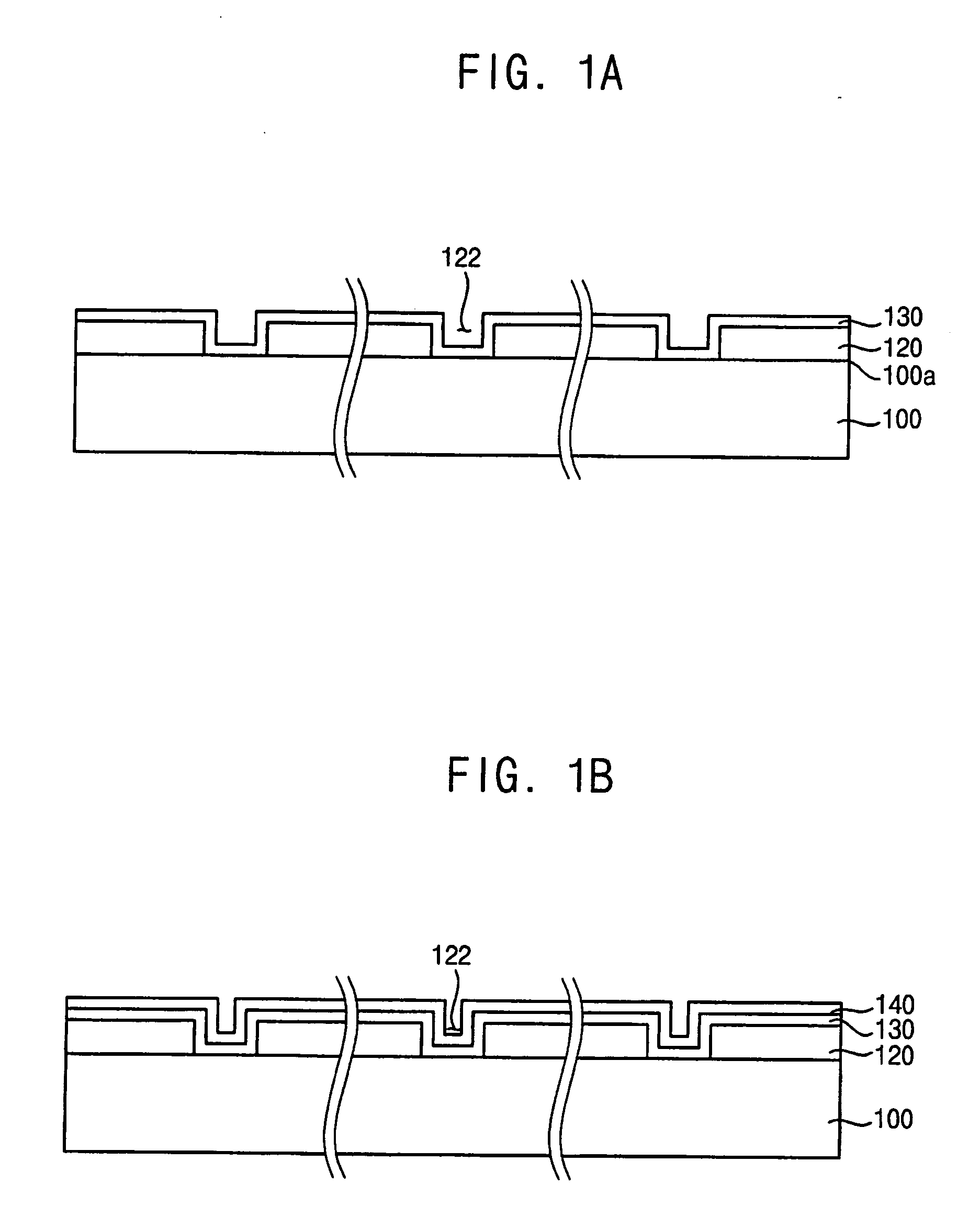
[0011]The method may further include forming an insulation layer between the substrate and the metal-based layer. The method may further include forming a contact hole through the insulation layer to partially expose the at least one conductive structure, the metal-based layer being conformally formed on the insulation layer. Forming the metal-based layer may include forming an anti-diffusion layer on the insulation layer. Forming the metal-based layer may include forming at least one metal layer on the insulation layer, the metal layer including one or more of tungsten (W), titanium (Ti), tantalum (Ta), tungsten nitride (WN), titanium nitride (TiN), and tantalum nitride (TaN). Forming the metal-based layer and the metal seed layer may include using an atomic layer deposition (ALD) process, a sputtering process, and / or a cyclic chemical vapor deposition (CVD) process.
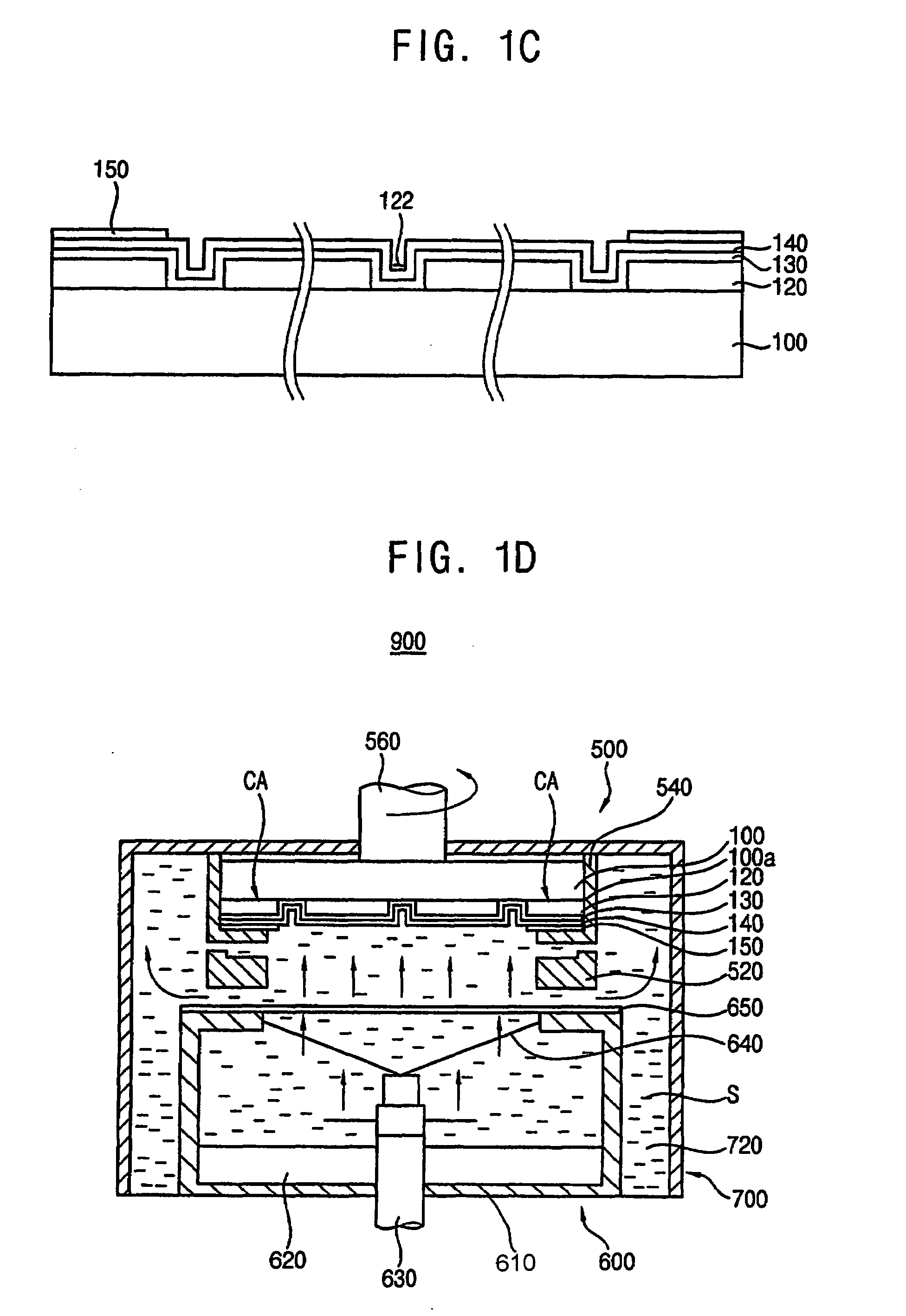
[0012]Forming the supplementary contact layer may include plating the supplementary metal on the metal seed layer along the peripheral portions of the substrate by an electroless plating (ELP) process using a plating solution, the plating solution including a mixture of a salt of the supplementary metal and a reducing agent having weaker reducing ability than the supplementary metal, and removing a residue of the plating solution from the peripheral portions of the substrate. Plating the supplementary metal on the metal seed layer by the ELP process may include securing the substrate to a rotation chuck, arranging an injection nozzle over the peripheral portion of the substrate, the injection nozzle being connected to a reservoir including the plating solution, and injecting the plating solution onto the metal seed layer while rotating the substrate. Plating the supplementary metal on the metal seed layer by the ELP process may include immersing the peripheral portion of the substrate into a reservoir including the plating solution, and rotating the reservoir while the substrate remains stationary. The supplementary metal may include one or more of copper (Cu), nickel (Ni), cobalt (Co), and palladium (Pd), and the reducing agent may include one or more of sodium borohydride, sodium hypophosphite, formalin, hydrazine sulfate, formate, dimethylamine borane (DMAB), diethylamine borane (DEAB), and triethylamine borane (TEAB). The metal seed layer and the supplementary contact layer may be formed of a substantially same material. Removing the residue of the plating solution includes supplying pure water onto the peripheral portions of the substrate.
[0013]Prior to plating the supplementary metal on the metal seed layer, the method may further include removing a native oxide layer from the metal seed layer, activating peripheral portions of the metal seed layer on corresponding peripheral portions of the substrates, and forming at least one plating nucleus on the peripheral portions of the metal seed layer. Activating the peripheral portions of the metal seed layer may include activating surface energy of the peripheral portions of the metal seed layer by a plasma treatment. The plasma treatment may be performed using one or more of nitrogen (N2), hydrogen (H2), oxygen (O2), and argon (Ar). Forming the plating nucleus may include immersing the activated metal seed layer into an aqueous solution with a nuclear material having smaller ionization tendency than the metal seed layer. The nuclear material may include palladium (Pd). Removing the native oxide layer from the metal seed layer may include injecting an alkaline solution onto the peripheral portions of the substrate. The alkaline solution may include an aqueous malic acid solution or an aqueous malonic acid solution. After forming the metal wiring layer, the method may further include forming a contact plug on the substrate by partially removing the metal-based layer and the metal wiring layer from the substrate, and forming a protective layer on the contact plug. Forming the protective layer may include forming a silver thin layer on the contact plug by a substitution reaction through an ELP process.

