
Semiconductor device

a technology of semiconductors and shielding devices, applied in emergency protection circuit arrangements, transistors, etc., can solve the problems of insufficient protection function, difficult to reduce the off-leak current of off-transistors, and increase the current consumption at standby during operation of the entire integrated circuit, etc., to achieve small manufacturing steps or occupation areas, the effect of protecting functions and sufficient esd protection functions

Active Publication Date: 2009-02-26
ABLIC INC
View PDF1 Cites 6 Cited by
  • Summary
  • Abstract
  • Description
  • Claims
  • Application Information

AI Technical Summary

Benefits of technology

[0015]Through the means as described above, there can be obtained a semiconductor device including an NMOS transistor for ESD protection provided with a sufficient ESD protection function while keeping the off-leak current small by preventing the generation of the leak current characteristic to the shallow trench isolation structure or by avoiding a region which generates leak current, without increasing manufacturing steps or an occupation area thereof.

Problems solved by technology

The width W of the off transistor is large as described above, and thus an off-leak current at standby during operation becomes larger, which leads to a problem of increase in the current consumption at standby during operation of the entire integrated circuit (IC) carrying the off transistor.
In particular, in the case of a semiconductor device in which a shallow trench is used for device isolation, there is a problem, in that an area adjacent to the shallow trench includes a region such as a crystal defect layer or the like which easily generates leak current, arising from the structure itself or a manufacturing method thereof, and hence it is difficult to reduce the off-leak current of the off transistor.
However, when the width W is made small to reduce the off-leak current of the off transistor, protection function cannot be sufficiently implemented.
Besides, in a semiconductor device in which a plurality of transistors are provided to cut the current path between the power line (Vdd) and the ground (Vss) as proposed in JP 2002-231886 A, an occupation area thereof increases because the semiconductor device includes the plurality of transistors, leading to an increase in cost for the semiconductor device.

Method used


Image

  • Semiconductor device
  • Semiconductor device
  • Semiconductor device

Examples


first embodiment

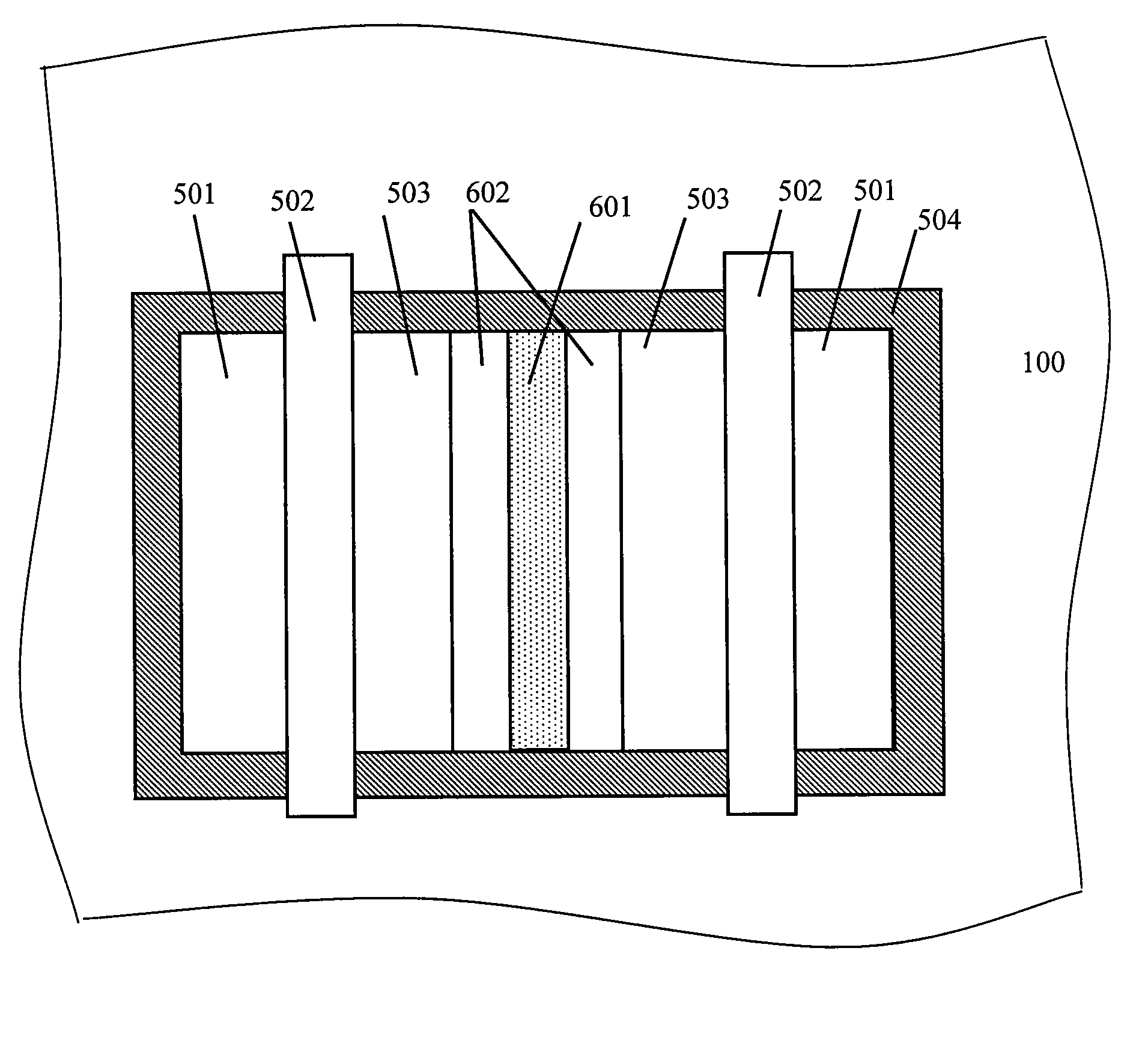
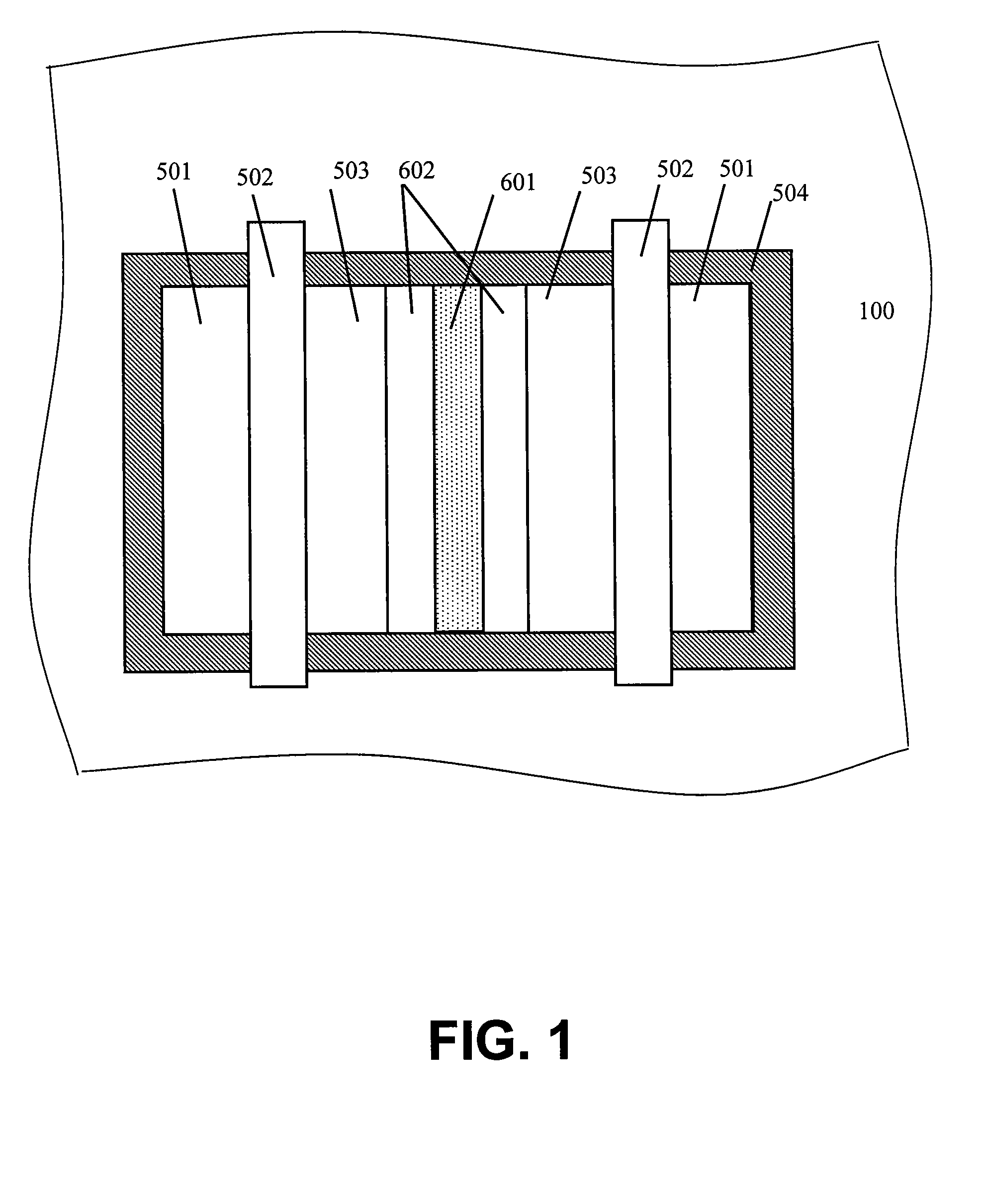
[0019]FIG. 1 is a schematic plan view showing an NMOS transistor for ESD protection of a semiconductor device according to a first embodiment of the present invention.

[0020]A pair of a source region 501 and a drain region 503 which are formed of an n-type heavily-doped impurity region are arranged on a p-type semiconductor substrate, a gate insulating film (not shown) made of a silicon oxide film or the like is placed between the source region 501 and the drain region 503, and a gate electrode 502 made of a polysilicon or the like is formed on an upper surface of the gate insulating film. A shallow trench structure is used for insulation from other elements, and a perimeter of the transistor is surrounded by a shallow trench isolation region 504.

[0021]In the embodiment of FIG. 1, two gate electrodes 502, and two pairs of the source region 501 and the drain region 503 each placed on either side of the gate electrode 502, are shown. In the vicinity of the drain regions 503, there is f...

second embodiment

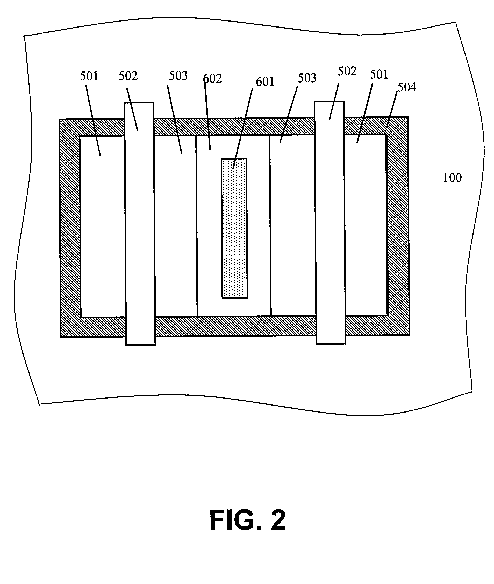
[0024]FIG. 2 is a schematic plan view showing an NMOS transistor for ESD protection of a semiconductor device according to a second embodiment of the present invention. The second embodiment is different from the first embodiment shown in FIG. 1 in that the n-type region 601 receiving a signal from the external connection terminal is wholly enclosed by the p-type region 602.

[0025]With this structure, the n-type region 601 receiving a signal from the external connection terminal has no portion in contact with the shallow trench isolation region 504, and thus there is no fear of a leak current in a portion adjacent to the shallow trench isolation region 504, which can be more effective at preventing the generation of the leak current compared with the first embodiment shown in FIG. 1. Other parts are denoted by the same reference numerals as FIG. 1, and thus their descriptions are omitted.

[0026]The embodiments of FIG. 1 and FIG. 2 show examples of the NMOS transistor for ESD protectio...


PUM


Abstract

In a semiconductor device including an n-type metal oxide semiconductor transistor for electrostatic discharge protection surrounded by a shallow trench for device isolation, in order to suppress the off-leak current in an off state, there is formed, in the vicinity of the drain region of the NMOS transistor for ESD protection, an n-type region receiving a signal from an external connection terminal via a p-type region in contact with the drain region of the NMOS transistor for ESD protection.

Description

[0001]This application claims priority under 35 U.S.C. §119 to Japanese Patent Application No. JP2007-215948 filed on Aug. 22, 2007, the entire content of which is hereby incorporated by reference.BACKGROUND OF THE INVENTION[0002]1. Field of the Invention[0003]The present invention relates to a semiconductor device including a metal oxide semiconductor (MOS) transistor. In particular, the present invention relates to a semiconductor device including an n-type MOS (NMOS) transistor isolated by a shallow trench structure as an electrostatic discharge (hereinafter, referred to as ESD) protective element.[0004]2. Description of the Related Art[0005]In a semiconductor device including MOS transistors, an off transistor, which is an NMOS transistor provided in an off-state whose gate potential is fixed to a ground (Vss), is used as an ESD protection element for preventing breakdown of an internal circuit due to static electricity supplied from a pad provided for external connection.[0006]...

Claims


Application Information

Patent Timeline
IPC IPC(8): H01L29/78
CPCH01L21/823418H01L29/78H01L29/0646H01L27/0266H01L27/04
Inventor TAKASU, HIROAKI
Owner ABLIC INC
Learn More