Resistive random access memory device

a random access and memory device technology, applied in semiconductor devices, digital storage, instruments, etc., can solve problems such as the loss of stored data when power is turned off, and achieve the effect of high enduran

Active Publication Date: 2009-02-26
SAMSUNG ELECTRONICS CO LTD
View PDF6 Cites 96 Cited by
  • Summary
  • Abstract
  • Description
  • Claims
  • Application Information

AI Technical Summary

Problems solved by technology

Dynamic random access memories (DRAMs) have the advantages of having high integration density and high response speed; however, have disadvantages in terms of losing stored data when power is turned off.

Method used


Image

  • Resistive random access memory device
  • Resistive random access memory device
  • Resistive random access memory device

Examples


Embodiment Construction

[0026]The present invention will now be described more fully with reference to the accompanying drawings in which exemplary embodiments of the invention are shown. In the drawings, the thicknesses of layers and regions are exaggerated for clarity, and like reference numerals refer to the like elements.

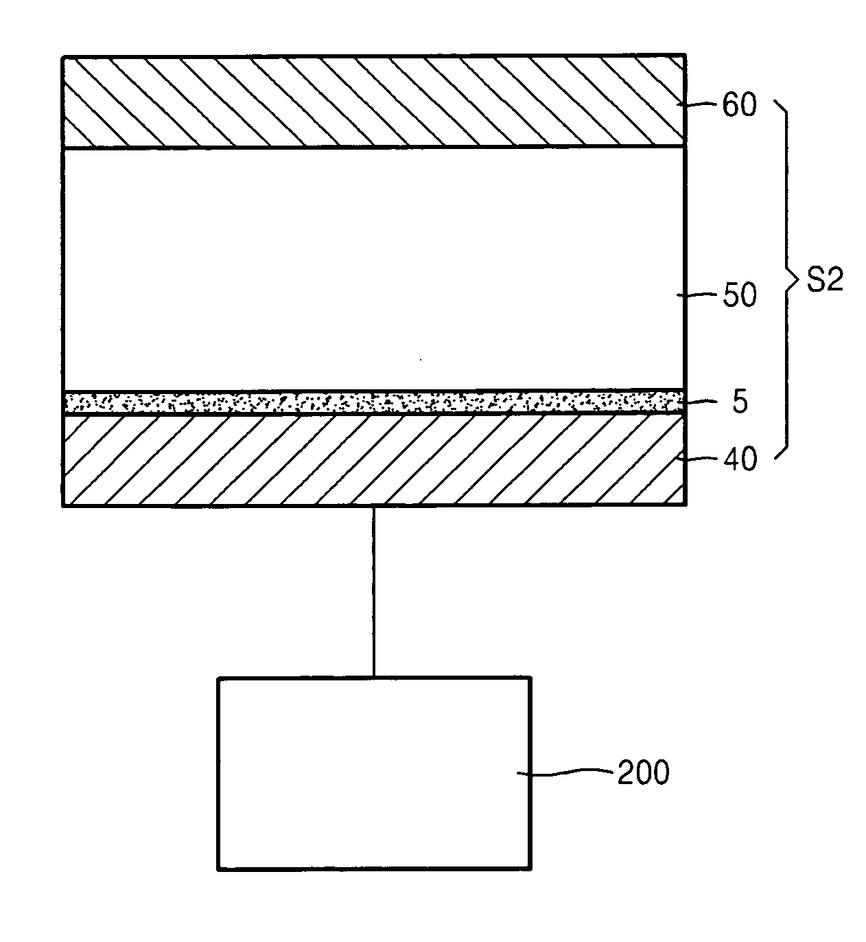
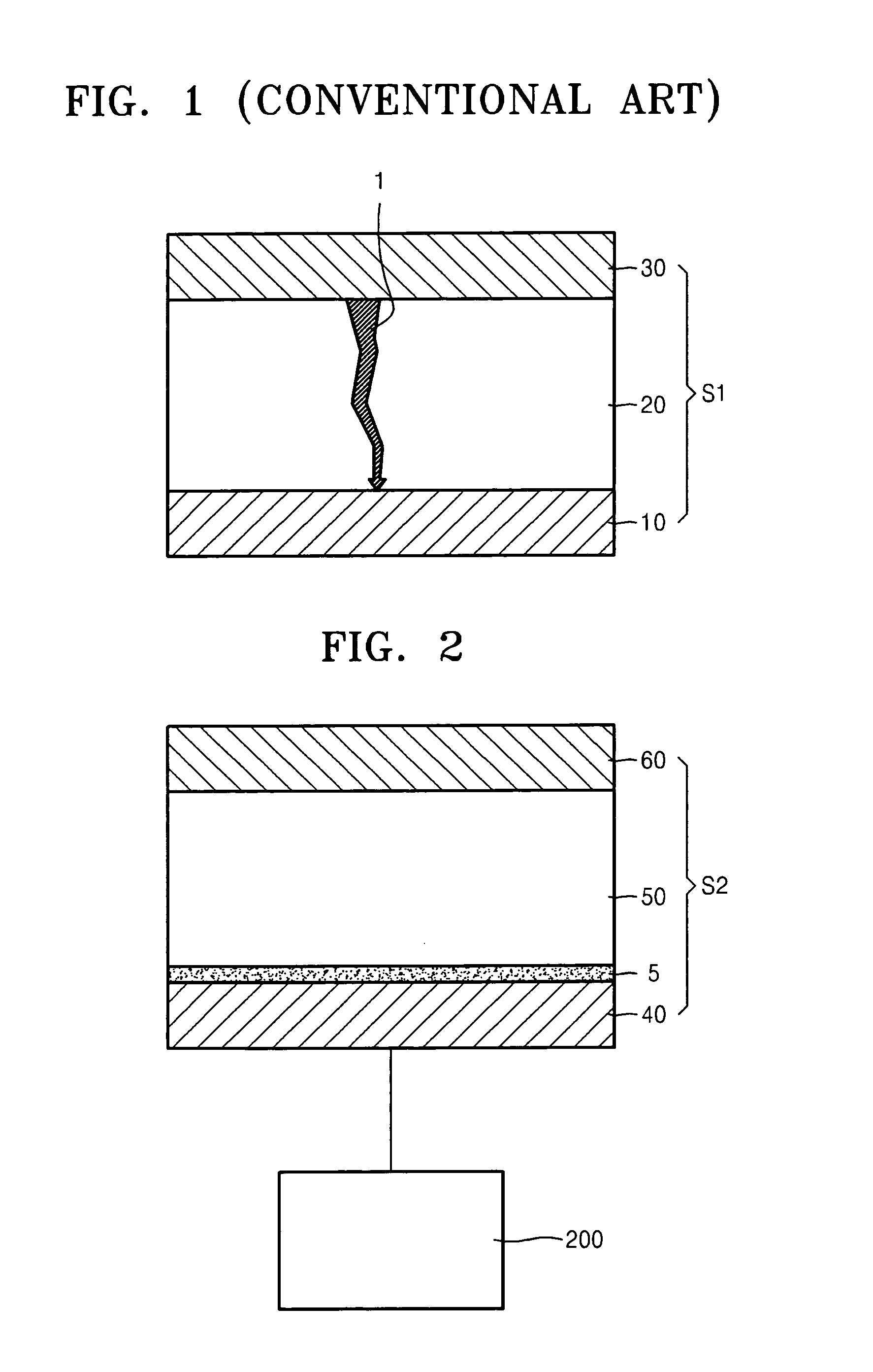
[0027]FIG. 2 is a cross-sectional view of a RRAM device according to an embodiment of the present invention.

[0028]Referring to FIG. 2, a switching device 200 is connected to a storage node S2. The switching device 200 can be a transistor or a diode. The storage node S2 includes a lower electrode 40, a resistance variable layer 50, and an upper electrode 60 that are sequentially formed. A diffusion blocking layer 5 is formed between the lower electrode 40 and the resistance variable layer 50 or between the resistance variable layer 50 and the upper electrode 60, for example, in the present embodiment, the diffusion blocking layer 5 is formed between the lower electrode 40 and the resist...


PUM


Abstract

Provided is a resistive random access memory device that includes a storage node connected to a switching device. The resistive random access memory device includes a first electrode, a resistance variable layer, and a second electrode which are sequentially stacked, wherein a diffusion blocking layer is formed between the first electrode and the resistance variable layer or between the resistance variable layer or / and the second electrode.

Description

CROSS-REFERENCE TO RELATED PATENT APPLICATION[0001]This application claims the benefit of Korean Patent Application No. 10-2007-0085558, filed on Aug. 24, 2007, in the Korean Intellectual Property Office, the disclosure of which is incorporated herein in its entirety by reference.BACKGROUND OF THE INVENTION[0002]1. Field of the Invention[0003]The present invention relates to a semiconductor device, and more particularly, to a resistive random access memory device.[0004]2. Description of the Related Art[0005]Dynamic random access memories (DRAMs) have the advantages of having high integration density and high response speed; however, have disadvantages in terms of losing stored data when power is turned off. Nonvolatile memory devices are memory devices in which the drawbacks of DRAMs do not apply, and thus, recently various nonvolatile memory devices have been proposed. Among such nonvolatile memory devices, resistive random access memories (RRAMs) have drawn attention as nonvolatil...

Claims


Application Information

Patent Timeline
Patent Type & Authority Applications(United States)
IPC IPC(8): G11C11/00
CPCG11C13/0007G11C2213/79G11C2213/51G11C2213/32H01L29/517
Inventor LEE, JUNG-HYUNLEE, MYOUNG-JAE
Owner SAMSUNG ELECTRONICS CO LTD
Why Eureka
Try Eureka