Electronic device manufacturing method using lds and electronic device manufactured by the method

a manufacturing method and electronic device technology, applied in the direction of printed circuit aspects, electrical apparatus casings/cabinets/drawers, substation equipment, etc., can solve the problems of reducing the size of a product, and high manufacturing cost, so as to improve the strength of the resin for lds

Inactive Publication Date: 2009-03-05
SAMSUNG ELECTRONICS CO LTD
View PDF22 Cites 27 Cited by
  • Summary
  • Abstract
  • Description
  • Claims
  • Application Information

AI Technical Summary

Benefits of technology

[0018]The present invention provides an electronic device manufacturing method using LDS and an elec

Problems solved by technology

However, there is a limit to the amount by which the size may be reduced by optimally arranging the parts having a large volume.
Therefore, there has recently been a tendency to reduce the size of a product by mounting parts in an external case of the product.
However, this method has a disadvantage in that the manufacturing cost may be high.
However, there is a disadvantage in that a poor circuit may be formed.
However, there may be limitations regarding the arrangement of the circuit within a device.
However, the cost of modifying the cir

Method used


Image

  • Electronic device manufacturing method using lds and electronic device manufactured by the method
  • Electronic device manufacturing method using lds and electronic device manufactured by the method
  • Electronic device manufacturing method using lds and electronic device manufactured by the method

Examples


Embodiment Construction

[0031]The invention is described more fully hereinafter with reference to the accompanying drawings, in which embodiments of the invention are shown. This invention may, however, be embodied in many different forms and should not be construed as limited to the embodiments set forth herein. Rather, these embodiments are provided so that this disclosure is thorough, and will fully convey the scope of the invention to those skilled in the art. Like reference numerals in the drawings denote like elements.

[0032]Hereinafter, exemplary embodiments of the present invention will be described with reference to the accompanying drawings.

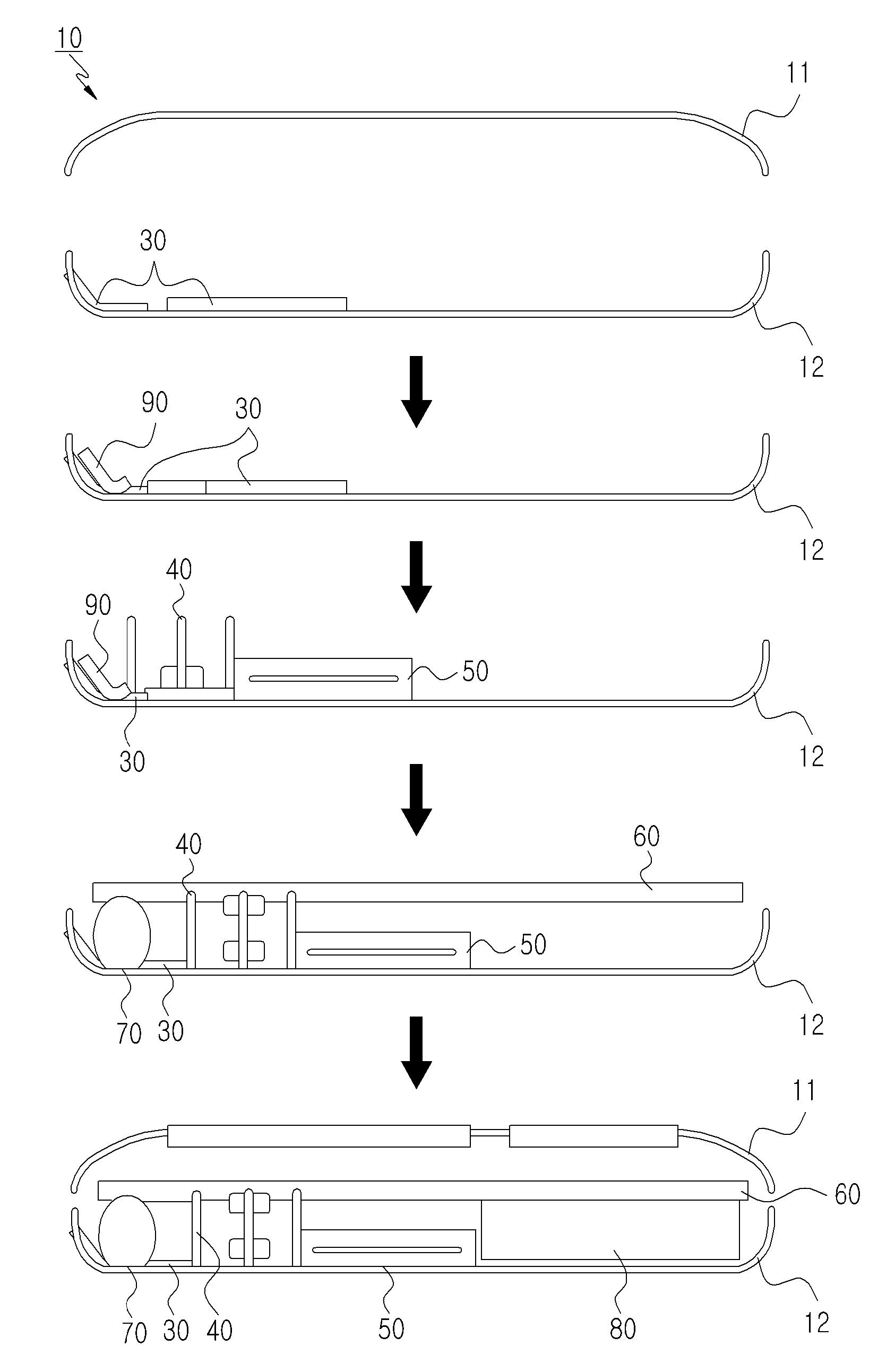
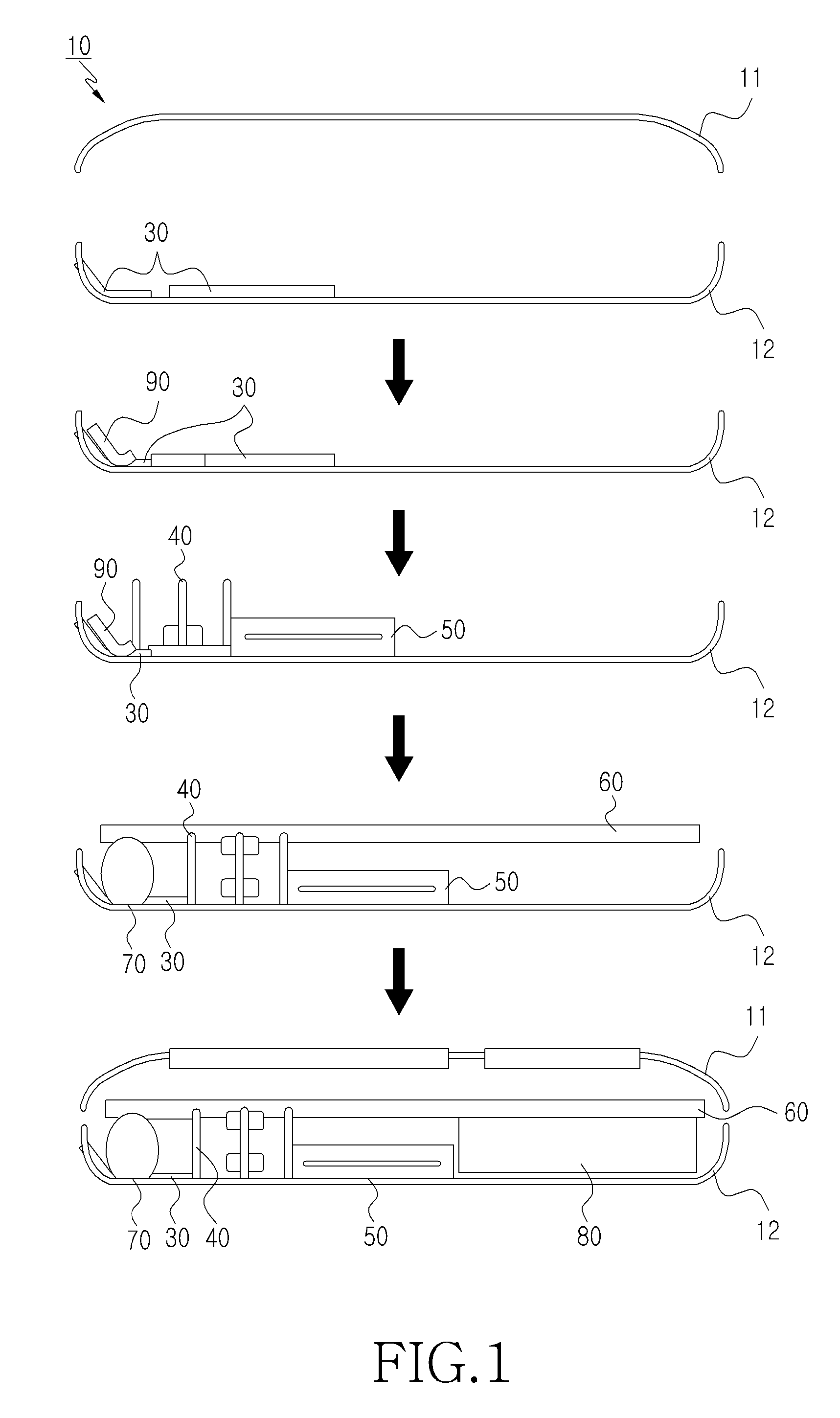
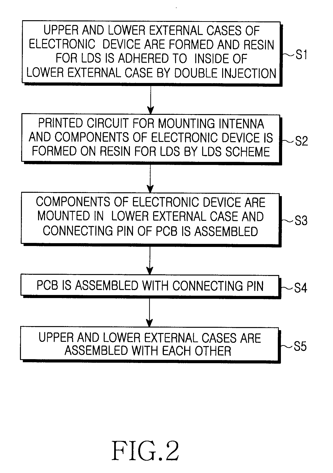
[0033]FIG. 1 and FIG. 3 show an electronic device 10 and 100, respectively, using Laser Direct Structuring (LDS) that includes upper and lower external cases 11 and 12. Resin 30 and 130 for LDS is adhered to an inner surface of the upper and lower external cases 11 and 12 by double injection or insert injection.

[0034]Herein, the resin 30 and 130 for an LDS is a...


PUM

PropertyMeasurementUnit
Adhesivityaaaaaaaaaa

Abstract

Disclosed is a method for manufacturing an electronic device using LDS and an electronic manufacturing by the method, in which resin for LDS is adhered to an inner surface of an external case by double injection or insert injection so as to implement a circuit. The electronic device using LDS includes upper and lower external cases, wherein resin for LDS is adhered to an inner surface of the lower external case by double injection or insert injection. Components of the electronic device are mounted on the resin, and the upper and lower external case are assembled with each other.

Description

CROSS REFERENCE TO RELATED APPLICATION[0001]This application claims priority from and the benefit of Korean Patent Application No. 10-2007-0089940, filed on Sep. 5, 2007, which is hereby incorporated by reference for all purposes as if fully set forth herein.BACKGROUND OF THE INVENTION[0002]1. Field of the Invention[0003]The present invention relates to an electronic device manufacturing method using laser direct structuring (LDS) and an electronic device manufactured by the method, in which resin for LDS is adhered to an inner surface of an external case of an electronic device by double injection or insert injection to implement a circuit.[0004]2. Discussion of the Background[0005]In general, one method of minimizing the size of an electronic product is to optimize the arrangement of its components. That is, the size of an electronic product may be reduced by optimizing the arrangement of parts mounted on a printed circuit board and optimizing the arrangement of parts that have a ...

Claims


Application Information

Patent Timeline
IPC IPC(8): H05K5/00B29C35/08
CPCH04M1/0249H05K1/0284H05K2203/107H05K2201/0999H05K3/185
Inventor CHOE, ICK-SUNGJEONG, HYUN-JUNGKIM, YOUNG-KIKANG, SHIN-CHULHONG, SOON-MINJANG, SE-YOUNGJIN, JAE-CHULHEO, GYUN
Owner SAMSUNG ELECTRONICS CO LTD
Why Eureka
Try Eureka