

Field effect transistor using oxide film for channel and method of manufacturing the same
a field effect transistor and oxide film technology, applied in transistors, semiconductor devices, electrical appliances, etc., can solve the problems of difficult formation of amorphous silicon tft, low thermal stability of organic semiconductors such as pentacene, and inability to realize practical devices, etc., to achieve high precision and reduce the variation in characteristic characteristics
- Summary
- Abstract
- Description
- Claims
- Application Information
AI Technical Summary
Benefits of technology
Problems solved by technology
Method used
Image

Examples
example 1
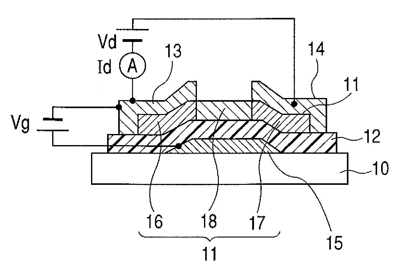
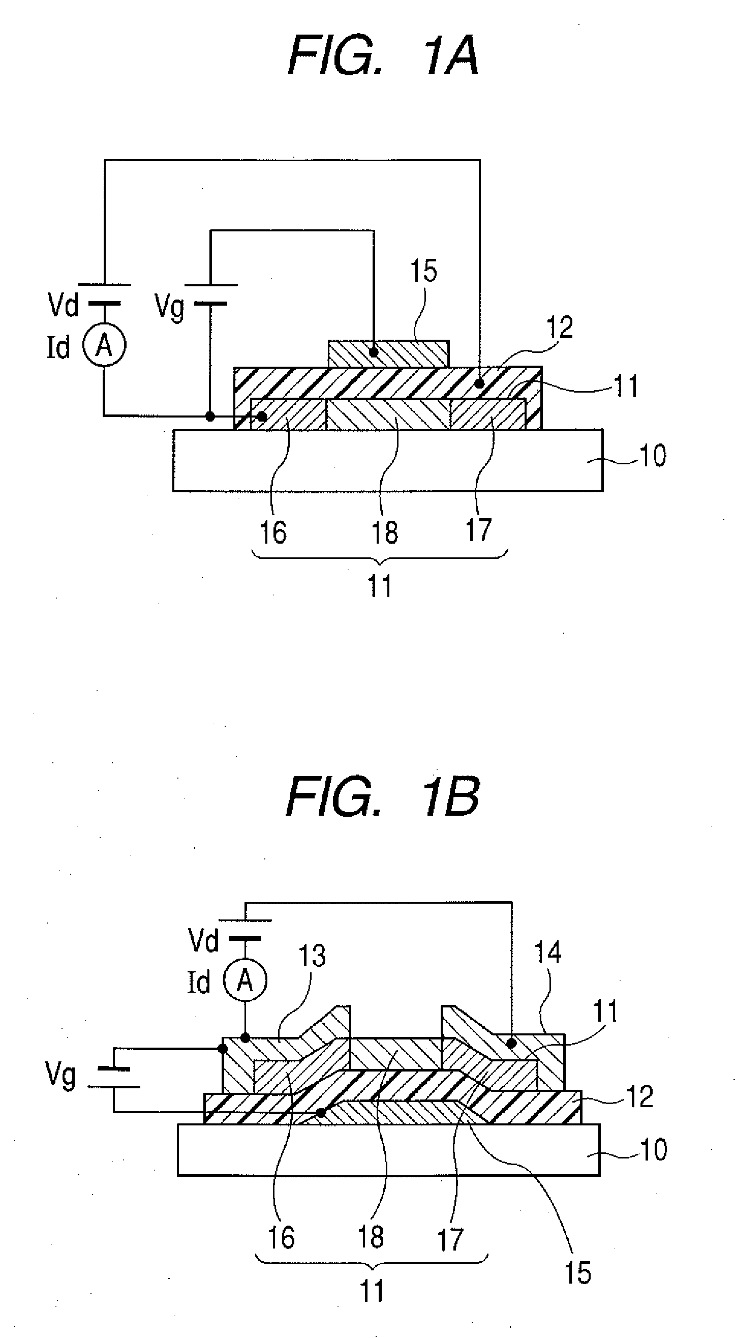
[0106]In this example, the top-gate TFT device having the coplanar structure as illustrated in FIG. 1A was manufactured.
[0107]With respect to a manufacturing method, the self-alignment method illustrated in FIGS. 3A and 3B was applied to this example.
[0108]An amorphous In—Ga—Zn—O oxide was used for the channel layer 11. A hydrogen ion implantation method was used to form the source part and the drain part.
[0109]First, the amorphous oxide film as the channel layer 11 was formed on the glass substrate 10 (manufactured by Corning Incorporated, 1737). In this example, the amorphous In—Zn—Ga—O oxide film was formed by radio frequency sputtering under a mixed atmosphere of argon gas and oxygen gas.
[0110]A sputtering apparatus for film formation as illustrated in FIG. 10 including a sample 51, a target 52, a vacuum pump 53, a vacuum gauge 54, a substrate holding means 55, gas flow rate control means 56 provided for the respective gas introduction systems, a pressure control means 57, and a...
example 2
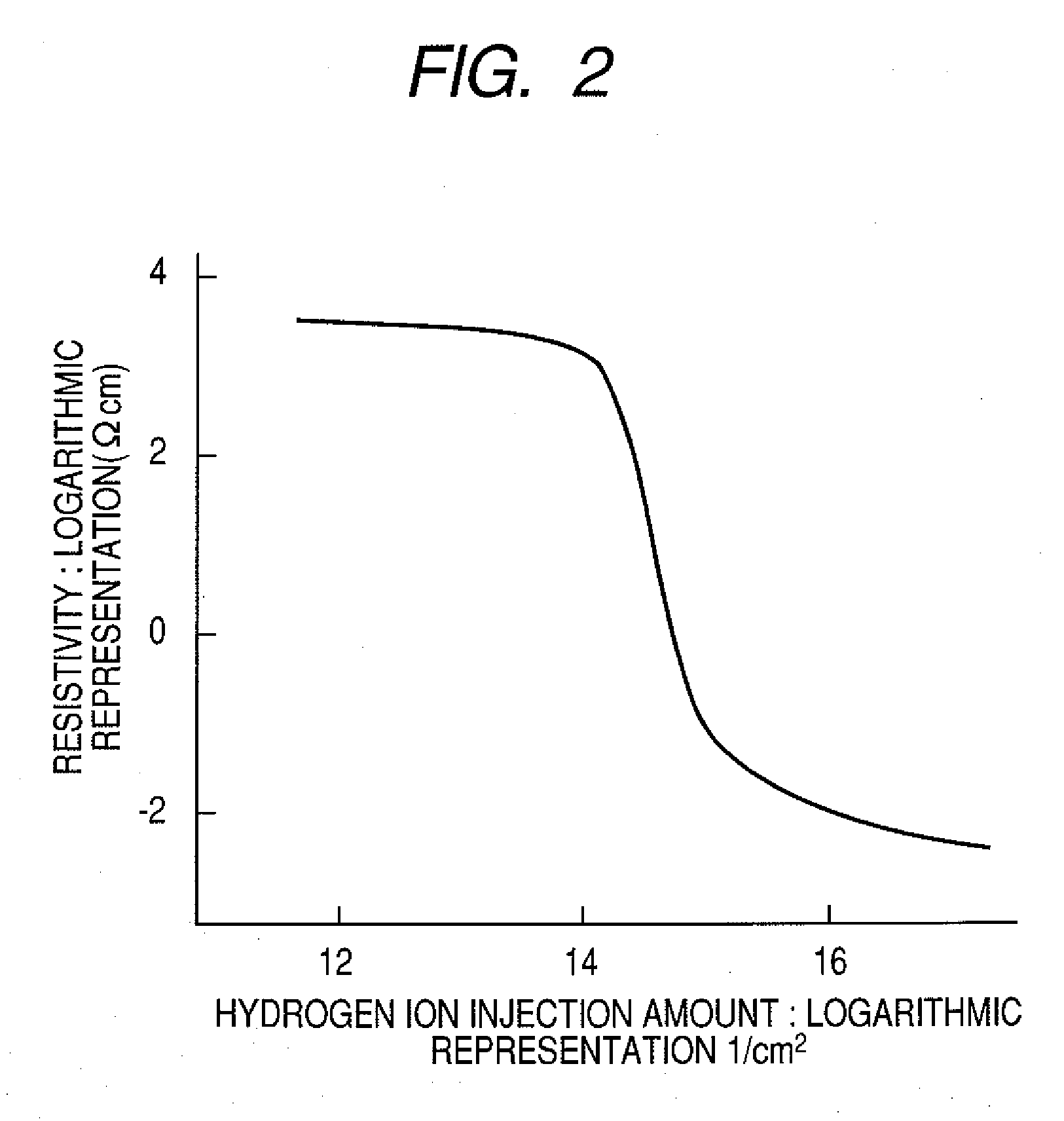
[0137]In this example, a structure and a manufacturing method were based on Example 1. However, a hydrogen implantation amount was controlled such that the hydrogen concentration of each of the source part and the drain part became approximately 1×10¹⁸ (1 / cm3).
[0138]In this example, the electric conductivity of each of the source part and the drain part was insufficient, and therefore the on-current was slightly smaller than that in Example 1. Electric conductivity of a specimen separately prepared at the above-mentioned hydrogen concentration was evaluated to obtain an electric conductivity of approximately 0.01 S / cm.
[0139]When the relatively low hydrogen concentration was applied to the source part and the drain part, the insulating layer 19, the source electrode, and the drain electrode were further provided as illustrated in FIG. 5A, so that the satisfactory transistor characteristics was able to be realized as in the case of Example 1. The hysteresis characteristic, the uniform...
example 3
[0140]This example is an example in which the bottom-gate TFT device having the coplanar structure as illustrated in FIG. 1B was manufactured.
[0141]In this example, the device was produced using the manufacturing method illustrated in FIGS. 4A to 4D. The self-alignment method was not used.
[0142]A channel layer made of amorphous In—Ga—Zn—O oxide was formed using a PLD method. The source part and the drain part were formed using hydrogen plasma processing.
[0143]First, the gate electrode 15 was patterned using a photolithography method and a lift-off method on a glass substrate 10 (manufactured by Corning Incorporated, 1737). The electrode was made of Ta and had a thickness of 50 nm.
[0144]Next, the gate insulating layer 12 was formed by patterning using a photolithography method and a lift-off method. The gate insulating layer was obtained by forming an HfO2 film in a thickness of 150 nm using a laser deposition method.
[0145]Further, an amorphous In—Zn—Ga—O oxide film which is the chan...
PUM
 Abstract
Description
Claims
Application Information