Methods of forming nano-coatings for improved adhesion between first level interconnects and epoxy under-fills in microelectronic packages and structures formed thereby

a technology of epoxy underfill and microelectronic package, which is applied in the direction of electrical apparatus, semiconductor devices, semiconductor/solid-state device details, etc., can solve the problems of poor adhesion between epoxy-based under-fill materials and copper interconnects, failures during post-assembling processes and/or reliability testing, and a greater amount of interconnect structures exposed

Inactive Publication Date: 2009-03-12
INTEL CORP
View PDF4 Cites 23 Cited by
  • Summary
  • Abstract
  • Description
  • Claims
  • Application Information

AI Technical Summary

Problems solved by technology

Poor adhesion between epoxy-based under-fill materials and copper interconnects may be of concern when used in lead-free packages.
Poor adhesion may result in failures during post assembly processes and / or during reliability testing.
This may result in a greater amount of the interconnect structure being exposed, which may then lead to poor adhesion with under-fill materials that may be dispensed during subsequent processing.

Method used


Image

  • Methods of forming nano-coatings for improved adhesion between first level interconnects and epoxy under-fills in microelectronic packages and structures formed thereby
  • Methods of forming nano-coatings for improved adhesion between first level interconnects and epoxy under-fills in microelectronic packages and structures formed thereby
  • Methods of forming nano-coatings for improved adhesion between first level interconnects and epoxy under-fills in microelectronic packages and structures formed thereby

Examples


Embodiment Construction

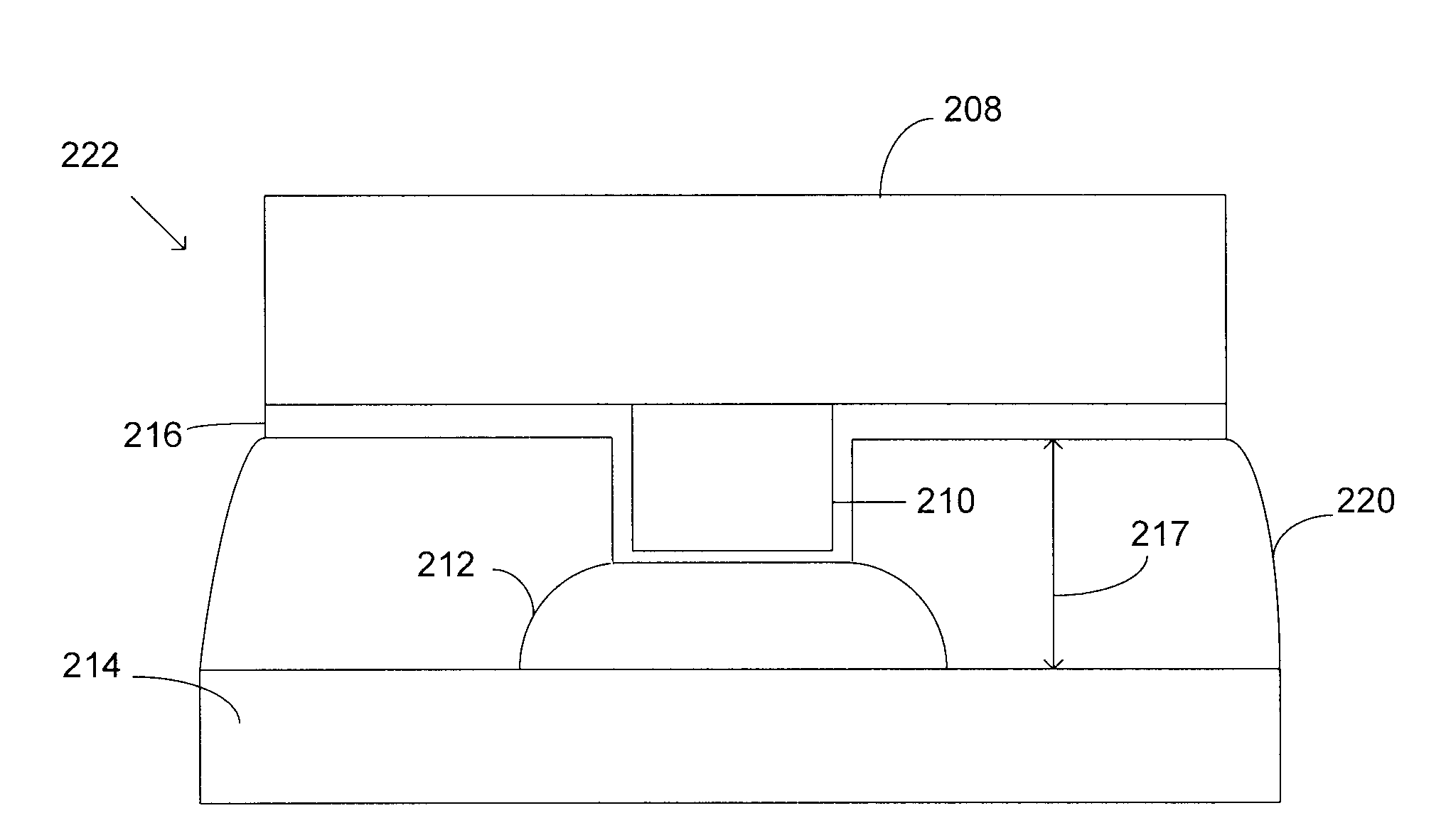
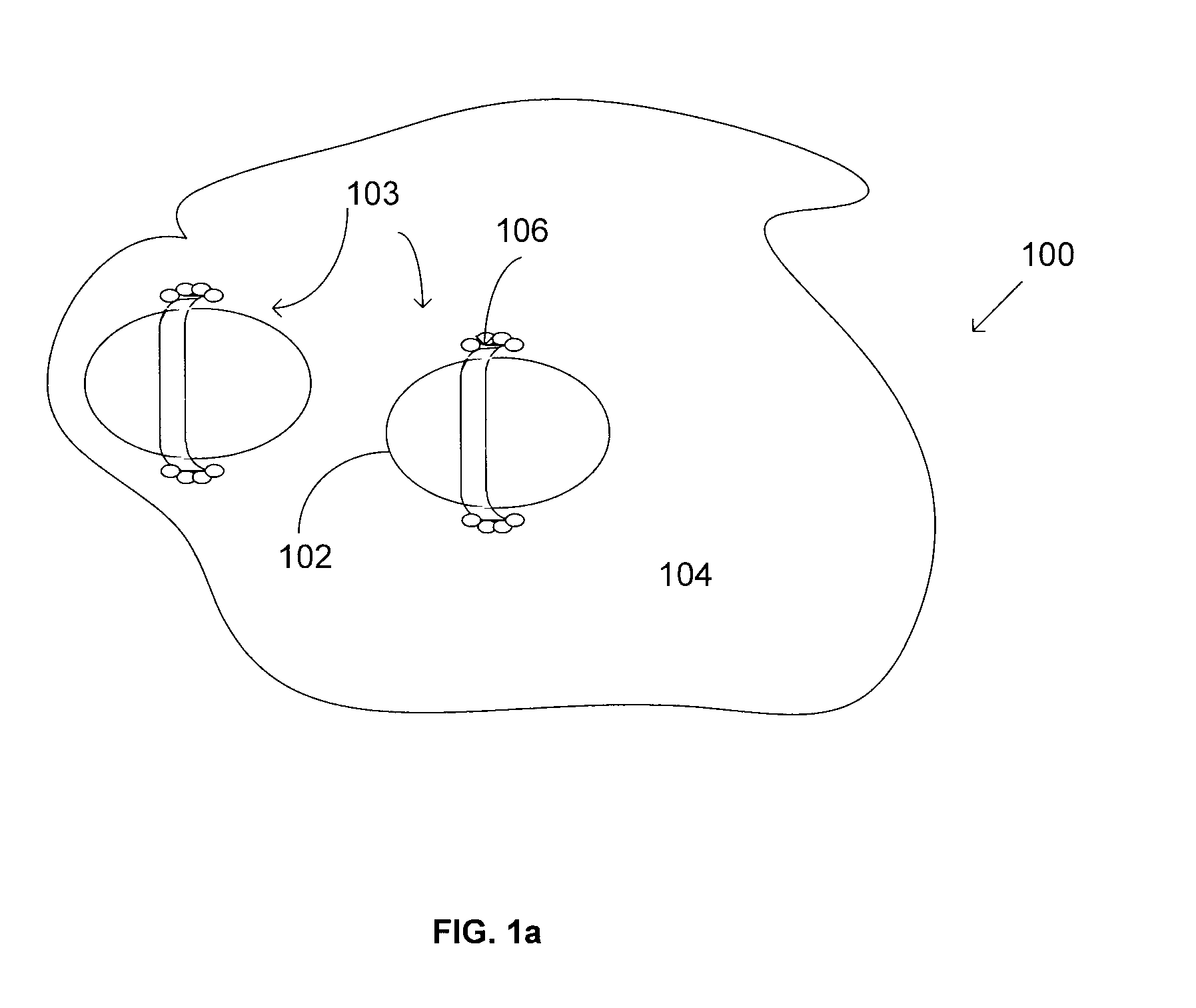
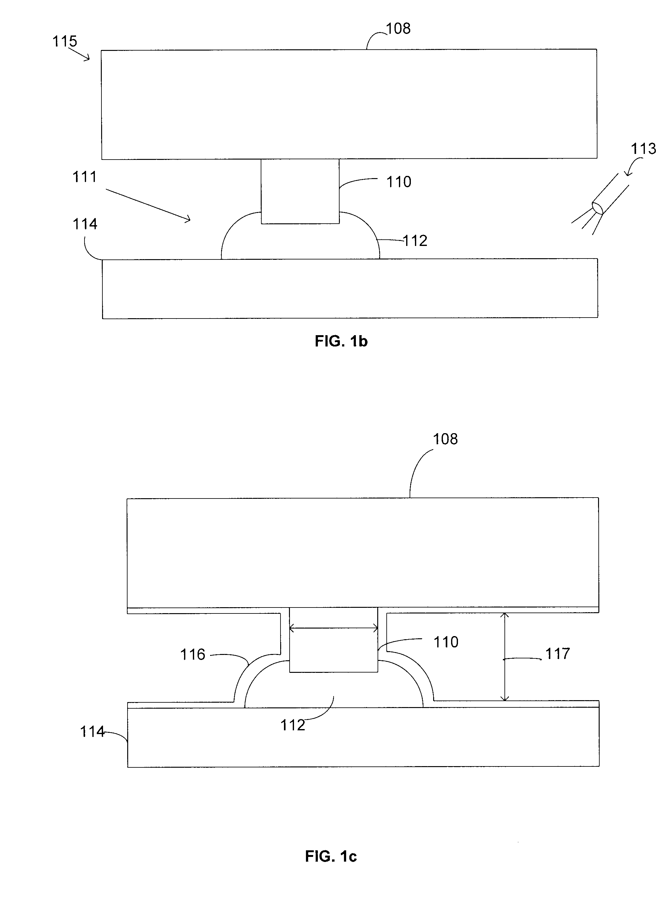
[0007]In the following detailed description, reference is made to the accompanying drawings that show, by way of illustration, specific embodiments in which the invention may be practiced. These embodiments are described in sufficient detail to enable those skilled in the art to practice the invention. It is to be understood that the various embodiments of the invention, although different, are not necessarily mutually exclusive. For example, a particular feature, structure, or characteristic described herein, in connection with one embodiment, may be implemented within other embodiments without departing from the spirit and scope of the invention. In addition, it is to be understood that the location or arrangement of individual elements within each disclosed embodiment may be modified without departing from the spirit and scope of the invention. The following detailed description is, therefore, not to be taken in a limiting sense, and the scope of the present invention is defined ...


PUM

PropertyMeasurementUnit
thicknessaaaaaaaaaa
thicknessaaaaaaaaaa
thicknessaaaaaaaaaa

Abstract

Methods and associated structures of forming microelectronic devices are described. Those methods may include coating an interconnect structure disposed on a die with a layer of functionalized nanoparticles, wherein the functionalized nanoparticles are dispersed in a solvent, heating the layer of functionalized nanoparticles to drive off a portion of the solvent, and applying an underfill on the coated interconnect structure.

Description

BACK GROUND OF THE INVENTION[0001]Poor adhesion between epoxy-based under-fill materials and copper interconnects may be of concern when used in lead-free packages. Poor adhesion may result in failures during post assembly processes and / or during reliability testing. In some cases, wicking of lead free solders (such as SnAg or SnAgCu, for example) may not occur along an entire surface of an interconnect structure, such as a copper bump for example. This may result in a greater amount of the interconnect structure being exposed, which may then lead to poor adhesion with under-fill materials that may be dispensed during subsequent processing.BRIEF DESCRIPTION OF THE DRAWINGS[0002]While the specification concludes with claims particularly pointing out and distinctly claiming that which is regarded as the present invention, the advantages of this invention can be more readily ascertained from the following description of the invention when read in conjunction with the accompanying drawi...

Claims


Application Information

Patent Timeline
Patent Type & Authority Applications(United States)
IPC IPC(8): H01L21/60H01L23/48
CPCH01L21/563H01L2224/2919H01L23/293H01L23/3157H01L24/11H01L24/13H01L24/81H01L24/83H01L2224/1182H01L2224/11827H01L2224/13111H01L2224/13147H01L2224/13687H01L2224/13693H01L2224/165H01L2224/73204H01L2224/814H01L2224/8192H01L2224/81948H01L2224/831H01L2224/83379H01L2924/01013H01L2924/01029H01L2924/01033H01L2924/01082H01L23/291H01L2224/81193H01L2224/16225H01L2924/0665H01L2924/014H01L2924/01006H01L2924/01005H01L2924/00014H01L2924/00H01L2924/3512H01L2224/05568H01L2224/05573
Inventor SANE, SANDEEPRARAVIKAR, NACHIKET
Owner INTEL CORP
Why Eureka
Try Eureka