
Method of forming contact plug of semiconductor device

a technology of contact plugs and semiconductor devices, which is applied in the manufacturing of semiconductor/solid-state devices, basic electric elements, electric devices, etc., can solve the problems of difficult to form drain contact holes and contact holes for high-voltage devices with desired sizes, photomask processes cannot be performed at the same time, etc., to achieve the effect of simplifying the process and reducing the prime cos

Active Publication Date: 2009-03-12
SK HYNIX INC
View PDF2 Cites 7 Cited by
  • Summary
  • Abstract
  • Description
  • Claims
  • Application Information

AI Technical Summary

Benefits of technology

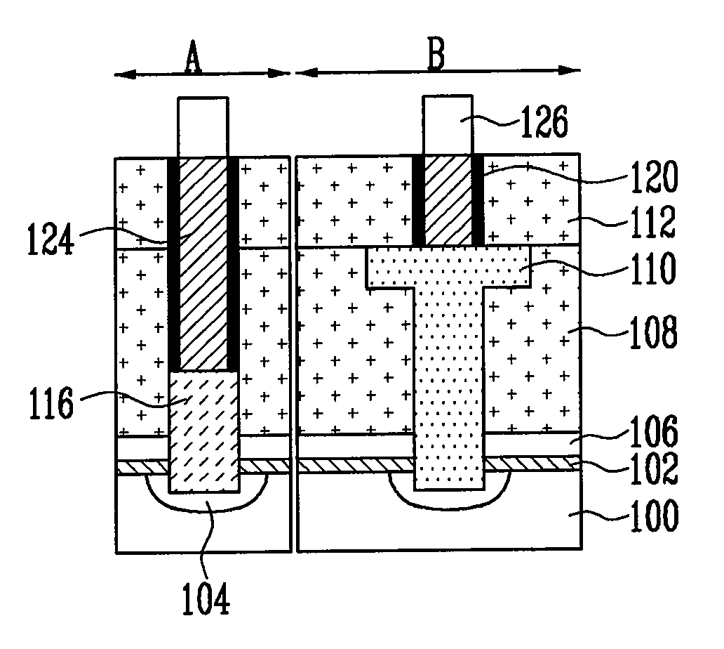
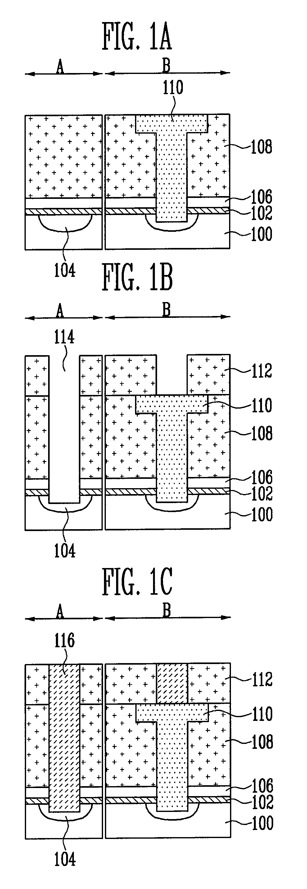
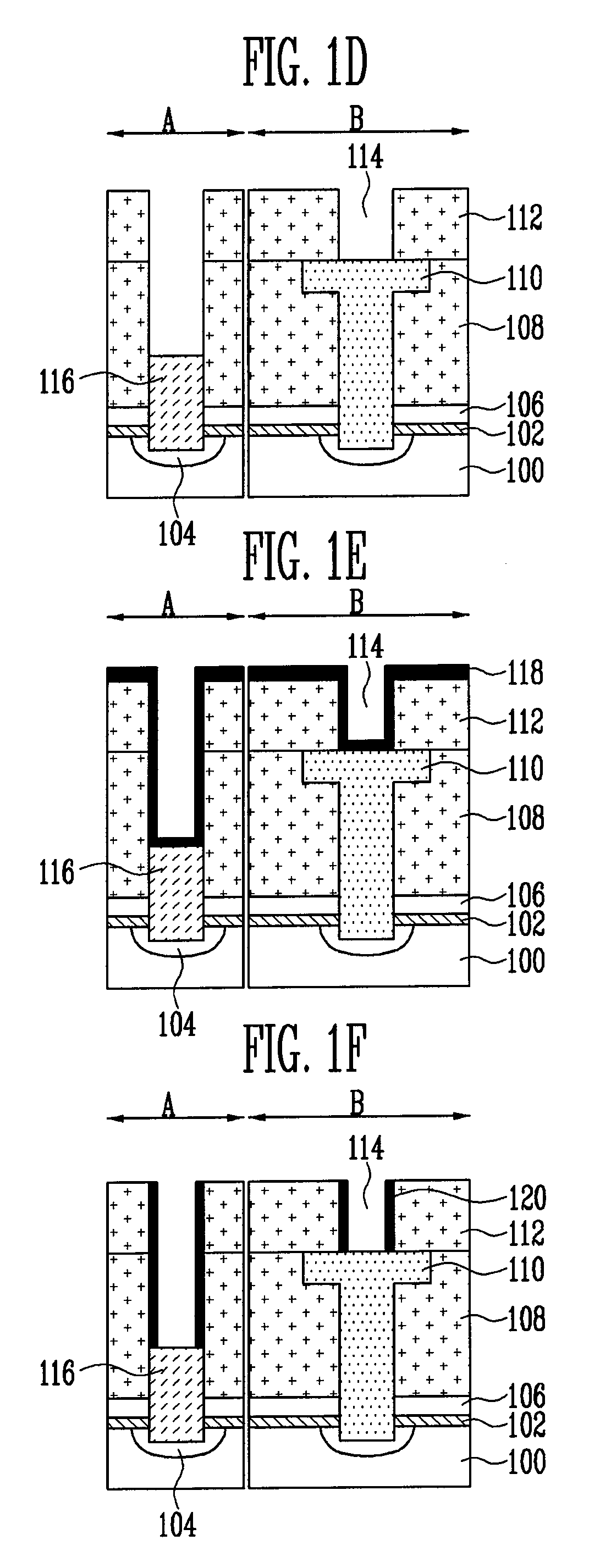
[0006]The present invention relates to a method of forming contact plugs of a semiconductor device, in which mask formation processes for defining contact holes of a cell region and a peri region are performed at the same time and the contact holes of the cell region and the contact holes of the peri region are gap-filled with the same material, thus simplifying the process and reducing the prime cost.

Problems solved by technology

As devices are miniaturized below 60 nm, a problem arises with some of the photomask processes.
When forming the drain contact plug of a cell region and the contact plug for a high voltage device of a peri region, these photomask processes cannot be performed at the same time.
If a mask formation process is performed on the basis of any one region, mask patterns formed on the other region deviate from the specs, making it difficult to form the drain contact hole and the contact hole for a high voltage device with a desired size.
Therefore, the process of forming the drain contact plug and the process of forming the contact plug for a high voltage device cannot be performed at the same time.
As described above, the process of forming the drain contact plug and the process of forming the contact plug for a high voltage device are not performed at the same time, but separately carried out due to the mask formation process problem and a difference in materials for gap-filling the drain contact hole and the contact hole for a high voltage device.
Accordingly, manufacturing costs for forming mask patterns are increased due to the added subsequent processes.

Method used


Image

  • Method of forming contact plug of semiconductor device
  • Method of forming contact plug of semiconductor device
  • Method of forming contact plug of semiconductor device

Examples


Embodiment Construction

[0012]A specific embodiment according to the present invention will be described with reference to the accompanying drawings. However, the present invention is not limited to the disclosed embodiment, but may be implemented in various ways. The embodiment is provided to complete the disclosure of the present invention and to allow those having ordinary skill in the art to understand the scope of the present invention. The present invention is defined by the category of the claims.

[0013]FIGS. 1A to 1I are cross-sectional views illustrating a method of forming contact plugs of a semiconductor device in accordance with an embodiment of the present invention. In the drawings, ‘A’ denotes a region in which drain contact plugs of a cell region are formed, and ‘B’ denotes a region in which contact plugs for low and high voltage devices, of a peri region, are formed.

[0014]Referring to FIG. 1A, there is provided a semiconductor substrate 100 in which a plurality of select lines (not shown), ...


PUM


Abstract

The present invention relates to a method of forming contact plugs of a semiconductor device. According to the method, a first insulating layer is formed over a semiconductor substrate in which a cell region and a peri region are defined and a first contact plug is formed in the peri region. The first insulating layer is etched using an etch process, thus forming contact holes through which junctions are exposed in the cell region and the first contact plug is exposed in the peri region. Second contact plugs are formed in the contact holes. The second contact plug formed within the contact hole of the peri region are removed using an etch process. A spacer is formed on sidewalls of the contact holes. Third contact plugs are formed within the contact holes.

Description

CROSS-REFERENCES TO RELATED APPLICATION[0001]The present application claims priority to Korean patent application number 10-2007-0091510, filed on Sep. 10, 2007, which is incorporated by reference in its entirety.BACKGROUND OF THE INVENTION[0002]The present invention relates to a semiconductor device and, more particularly, to a method of forming contact plugs of a semiconductor device, which can simplify the contact plug formation process and reduce the prime cost.[0003]As devices are miniaturized below 60 nm, a problem arises with some of the photomask processes. When forming the drain contact plug of a cell region and the contact plug for a high voltage device of a peri region, these photomask processes cannot be performed at the same time.[0004]This is because a drain contact hole and a contact hole for a high voltage device have different shapes and sizes. If a mask formation process is performed on the basis of any one region, mask patterns formed on the other region deviate f...

Claims


Application Information

Patent Timeline
Patent Type & Authority Applications(United States)
IPC IPC(8): H01L21/768
CPCH01L21/76816H01L21/76897H01L21/76877H01L21/76831H01L21/28
Inventor KIM, JAE HEON
Owner SK HYNIX INC
Learn More