Light-Emitting Element, Light-Emitting Device, and Electronic Device

a technology of light-emitting elements and electronic devices, which is applied in the direction of discharge tubes/lamp details, organic semiconductor devices, discharge tubes/lamp details, etc., can solve the problems of short lifetime of light-emitting elements and poor durability of hole-blocking layers, and achieve long lifetime and suppress the effect of carrier balance change with tim

Active Publication Date: 2009-03-19
SEMICON ENERGY LAB CO LTD
View PDF33 Cites 43 Cited by
  • Summary
  • Abstract
  • Description
  • Claims
  • Application Information

AI Technical Summary

Benefits of technology

[0013]In view of the foregoing, it is an object of the present invention to provide a light-emitting element having long lifetime. In addition, it is another object to provide a light-emitting device and an electronic device having long lifetime.
[0014]As a result of diligent studies, the present inventors have found that a light-emitting element with high light emission efficiency and a light-emitting element having long lifetime can be obtained by providing a layer for controlling the carrier transport.
[0039]In a light-emitting element of the present invention, a layer for controlling the carrier transport is provided, and a change with time of carrier balance can be suppressed. Thus, a light-emitting element having long lifetime can be obtained.
[0040]Furthermore, by applying the light-emitting element of the present invention to a light-emitting device and an electronic device, a light-emitting device and an electronic device having long lifetime can be obtained.

Problems solved by technology

However, as disclosed in Reference 1, the hole-blocking layer has poor durability, and the light-emitting element has short lifetime.

Method used


Image

  • Light-Emitting Element, Light-Emitting Device, and Electronic Device
  • Light-Emitting Element, Light-Emitting Device, and Electronic Device
  • Light-Emitting Element, Light-Emitting Device, and Electronic Device

Examples


embodiment mode 1

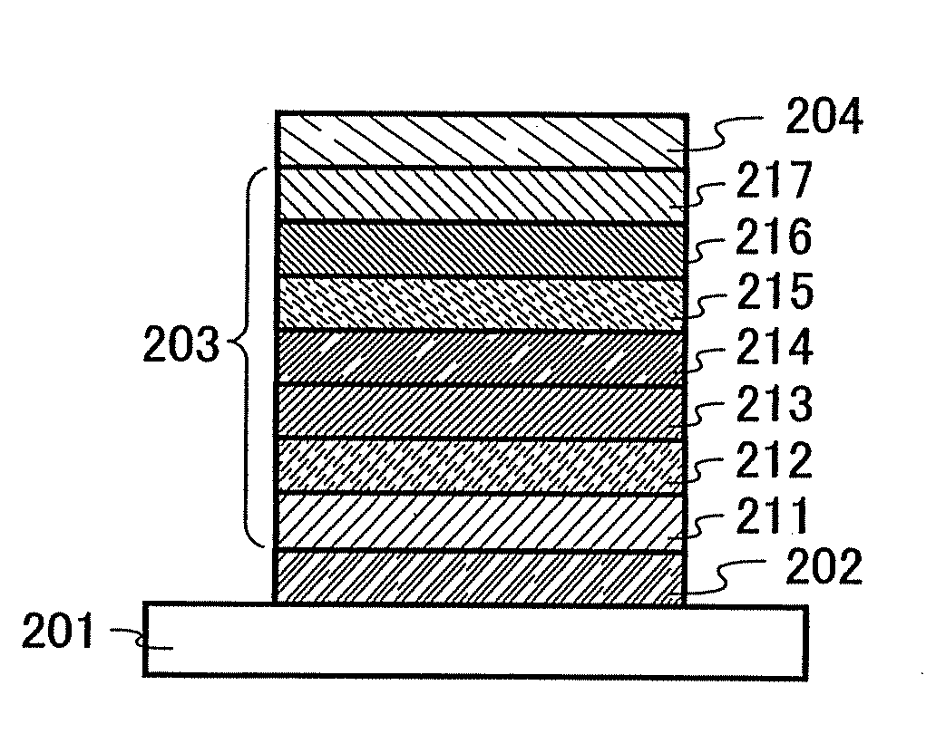
[0068]A light-emitting element of the present invention will be described below with reference to FIGS. 1A to 1D. A light-emitting element of the present invention includes a layer for controlling the hole transport and a layer for controlling the electron transport.

[0069]The light-emitting element of the present invention has a plurality of layers between a pair of electrodes. The plurality of layers are stacked by combining layers formed from a substance with a high carrier-injecting property or a substance with a high carrier-transporting property so that a light-emitting region is formed at a place apart from the electrodes, in other words, carriers are recombined at a portion apart from the electrodes.

[0070]In this embodiment mode, a light-emitting element includes a first electrode 202, a second electrode 204, and an EL layer 203 provided between the first electrode 202 and the second electrode 204. Note that in this embodiment mode, description is made on the assumption that ...

embodiment mode 2

[0160]This embodiment mode will describe the case where a layer having a different structure from that described in Embodiment Mode 1 is used for the layer for controlling the electron transport. Except for the layer for controlling the electron transport, the structure described in Embodiment Mode 1 can be used.

[0161]The layer 215 for controlling the electron transport described in this embodiment mode contains a third organic compound and a fourth organic compound, and the weight percent of the third organic compound is higher than that of the fourth organic compound. That is, the fourth organic compound is dispersed in the third organic compound. In addition, the layer for controlling the electron transport is preferably provided between the light-emitting layer 214 and the second electrode 204.

[0162]In the case where the layer for controlling the electron transport is provided between the light-emitting layer and the second electrode functioning as a cathode, the third organic c...

embodiment mode 3

[0197]In this embodiment mode, a light-emitting element in which a plurality of light-emitting units according to the present invention are stacked (hereinafter, referred to as a stacked type element) will be described with reference to FIG. 7. The light-emitting element is a stacked-type light-emitting element including a plurality of light-emitting units between a first electrode and a second electrode. A structure similar to that described in Embodiment Modes 1 and 2 can be used for each light-emitting unit. In other words, the light-emitting element described in Embodiment Mode 2 is a light-emitting element having one light-emitting unit. In this embodiment mode, a light-emitting element having a plurality of light-emitting units will be described.

[0198]In FIG. 7, a first light-emitting unit 511 and a second light-emitting unit 512 are stacked between a first electrode 501 and a second electrode 502. As the first electrode 501 and the second electrode 502, an electrode similar t...


PUM


Abstract

It is an object to provide a light-emitting element having long lifetime. A light-emitting element is provided, in which a light-emitting layer, a first layer, and a second layer are provided between a first electrode and a second electrode; the first layer is provided between the light-emitting layer and the first electrode; the second layer is provided between the light-emitting layer and the second electrode; the first layer is a layer for controlling the hole transport; the second layer is a layer for controlling the electron transport; and light emission is obtained from the light-emitting layer by applying voltage to the first electrode and the second electrode such that the potential of the first electrode is higher than that of the second electrode.

Description

BACKGROUND OF THE INVENTION[0001]1. Field of the Invention[0002]The present invention relates to current excitation type light-emitting elements. Further, the present invention relates to light-emitting devices and electronic devices including the light-emitting elements.[0003]2. Description of the Related Art[0004]In recent years, research and development have been actively conducted on light-emitting elements utilizing electroluminescence. As a basic structure of these light-emitting elements, a structure in which a light-emitting substance is interposed between a pair of electrodes is used. By applying voltage to these elements, light emission can be obtained from the light-emitting substance.[0005]Compared to liquid crystal displays, such light-emitting elements are of self-light-emitting type and have advantages such as high visibility of pixels and no need of backlights. Thus, the light-emitting elements are suitable for flat panel display elements. In addition, such light-emi...

Claims


Application Information

Patent Timeline
Patent Type & Authority Applications(United States)
IPC IPC(8): H01J1/63
CPCH01L51/001H01L51/0031H01L51/0059H01L51/006H01L2251/308H01L51/0072H01L51/0081H01L51/5052H01L51/007H10K71/164H10K71/70H10K85/6565H10K85/631H10K85/633H10K85/6572H10K85/324H10K50/155H10K50/165H10K2102/103H05B33/14H05B33/20H10K99/00H10K50/11
Inventor SUZUKI, TSUNENORISHITAGAKI, SATOKOSEO, SATOSHI
Owner SEMICON ENERGY LAB CO LTD
Why Eureka
Try Eureka