Cof package and tape substrate used in same

a technology of cof package and tape substrate, which is applied in the direction of semiconductor/solid-state device details, electrical apparatus, semiconductor devices, etc., can solve the problems of insufficient size reduction of semiconductor elements and significant increase of semiconductor elements, and achieve high reliability

Active Publication Date: 2009-03-26
LAPIS SEMICON CO LTD
View PDF5 Cites 12 Cited by
  • Summary
  • Abstract
  • Description
  • Claims
  • Application Information

AI Technical Summary

Benefits of technology

[0012]A COF package of the present invention and a tape substrate employed therein can contribute to a size reduction in a semiconductor chip and hold high reliability by taking the constitution of the invention.

Problems solved by technology

Respective companies or manufacturers involve a problem that since the recent driver needs to form so many wiring areas inside the semiconductor element in order to meet these demands, the area of the semiconductor element increases significantly.
Under the stereotype that first connecting terminals are formed at a peripheral portion on the semiconductor element in particular, the size reduction in the semiconductor element was insufficient.

Method used


Image

  • Cof package and tape substrate used in same
  • Cof package and tape substrate used in same
  • Cof package and tape substrate used in same

Examples


first preferred embodiment

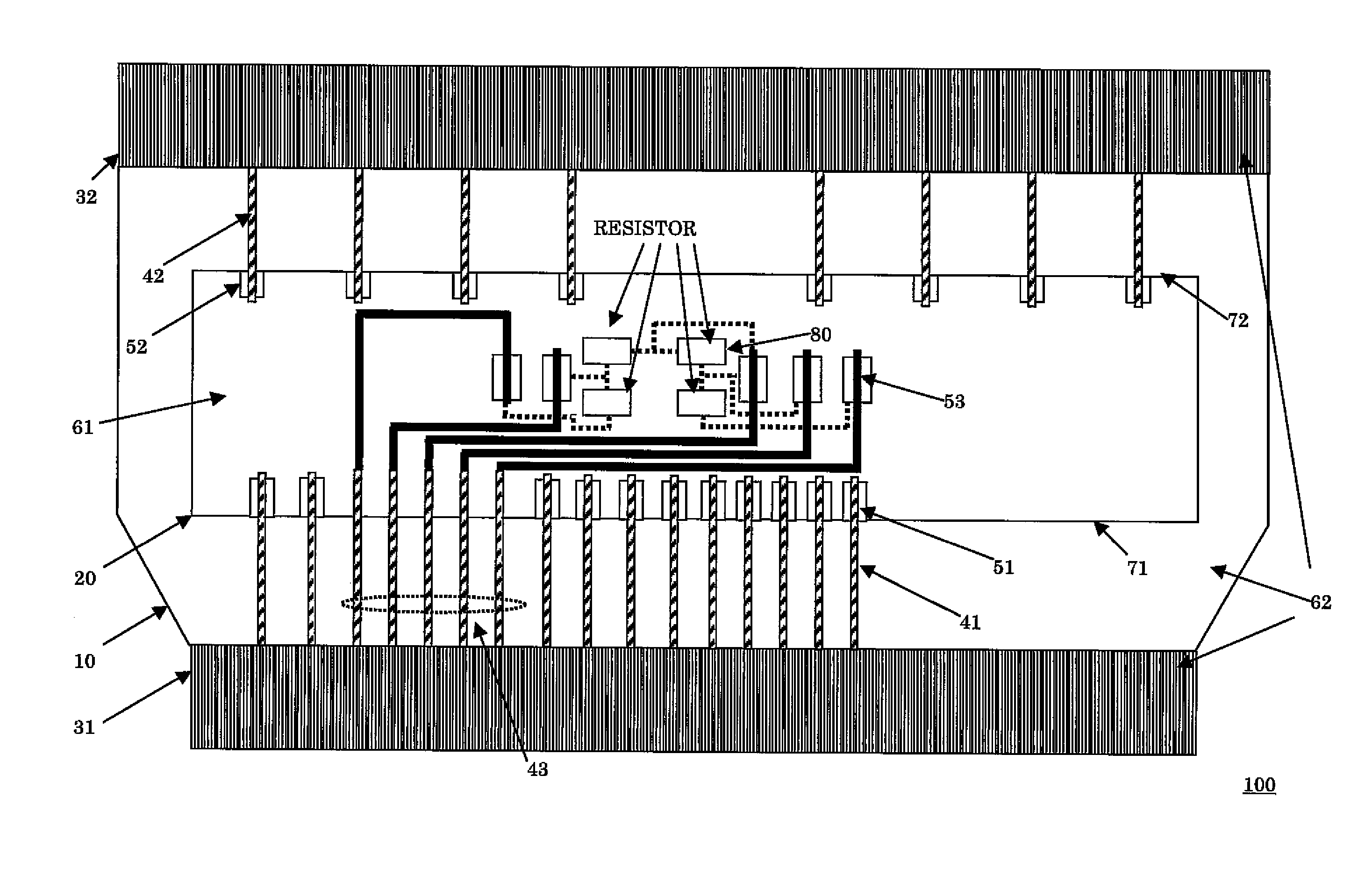
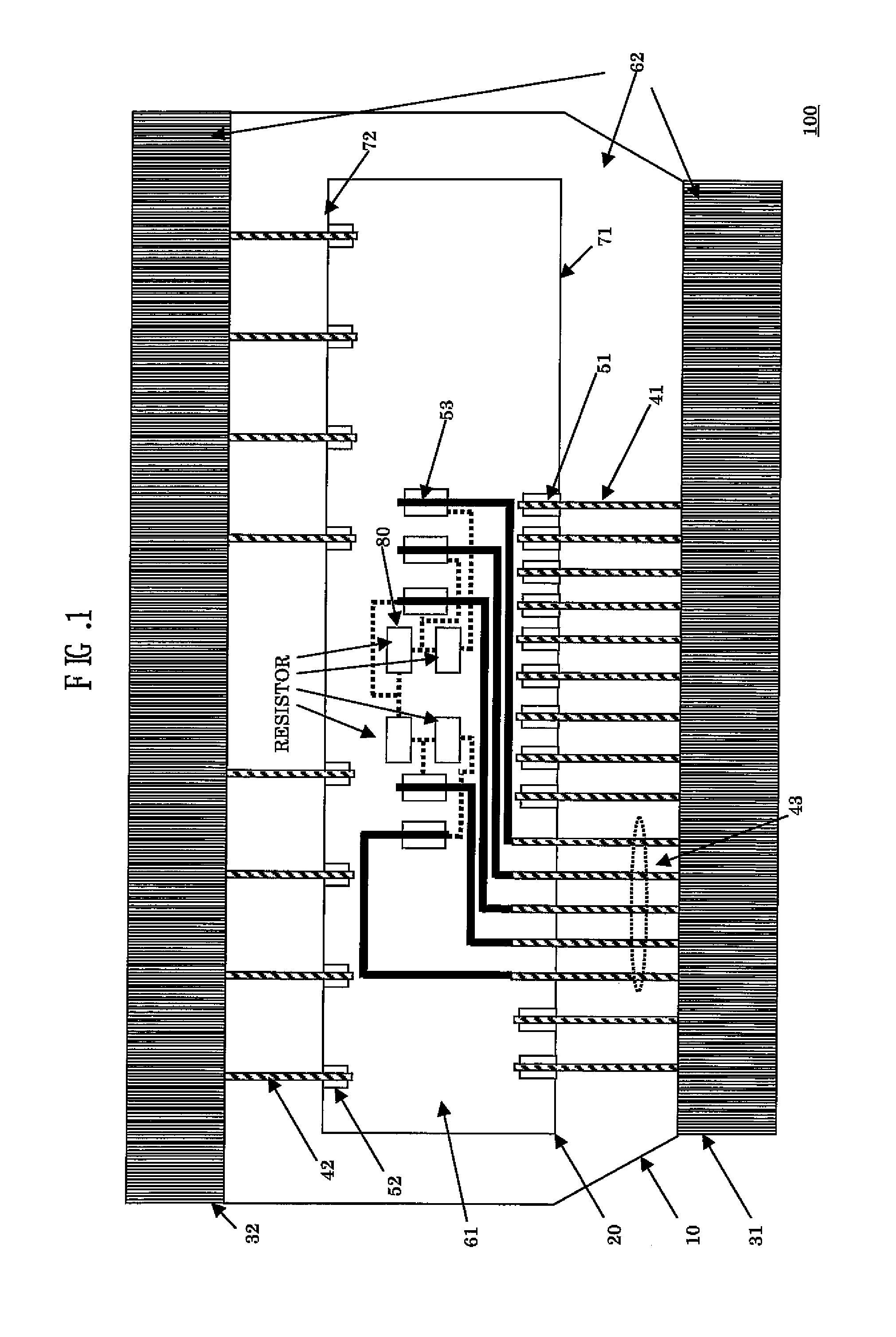
[0018]FIG. 1 is a conceptual diagram showing a COF package 100 according to a first embodiment of the present invention. The configuration of the present embodiment will be explained using FIG. 1. In the COF package 100, a rectangular semiconductor chip 20 is mounted on a tape substrate 10 in such a manner that a circuit forming surface of the semiconductor chip 20 is opposite to the tape substrate 10. The semiconductor chip 20 is generally sealed with an unillustrated sealing or encapsulating resin.

[0019]The tape substrate 10 includes, as minimum constituent requirements, external input terminals 31, external output terminals 32, input wirings 41 each corresponding to a first wiring pattern, output wirings 42 each corresponding to a second wiring pattern, and internal input wirings 43 each corresponding to a third wiring pattern. The semiconductor chip 20 is equipped with, as minimum constituent requirements, input electrodes 51 each corresponding to a first electrode, output elect...

second preferred embodiment

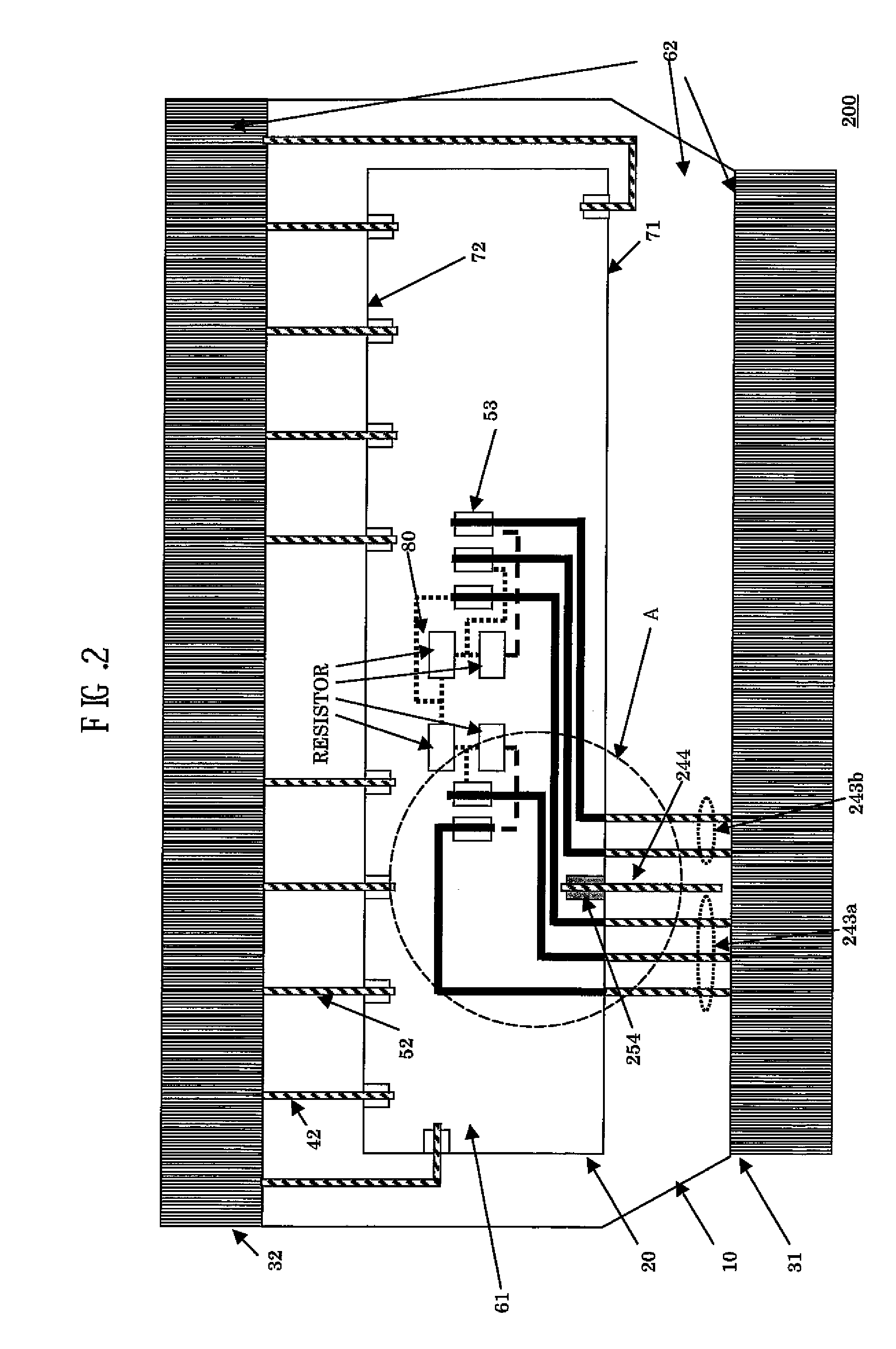
[0024]FIG. 2 shows a COF package according to a second embodiment of the present invention. FIG. 3 is a detailed diagram of a portion A shown in FIG. 2. The second embodiment will be explained below using FIGS. 2 and 3. Portions or elements different from those employed in the first embodiment will be explained in the following description.

[0025]As shown in FIG. 2, the invention of the second embodiment features that a dummy wiring 244 corresponding to a fourth wiring pattern is disposed between internal input wirings 243a and internal input wirings 243b in a tape substrate 10, and a dummy electrode 254 is disposed in a semiconductor chip 20.

[0026]The details of the second embodiment will be explained using FIG. 3. Part of the COF package is shown in FIG. 3. Areas are respectively formed or defined within a chip mounting area 61 provided on the tape substrate 10. A plurality of input electrode connecting areas 310 are defined along a first side 71. A plurality of wiring passage area...


PUM


Abstract

The present invention provides a COF package which comprises a tape substrate including a plurality of external input terminals and a plurality of external output terminals provided in a chip non-mounting area, a plurality of input wirings connected to the external input terminals respectively, a plurality of output wirings connected to the external output terminals respectively, a plurality of internal input wirings which are provided from the chip non-mounting area to a chip mounting area and provided between the input wirings and which are connected to the external input terminals, respectively, and a dummy wiring provided from the chip non-mounting area to the chip mounting area and provided between the internal input wirings; and a semiconductor chip including a plurality of input electrodes connected to the input wirings respectively, a plurality of output electrodes connected to the input wirings respectively, internal input electrodes connected to the internal input wirings respectively, and a dummy electrode provided with being spaced from each input electrode along one side lying over a chip surface, and connected to the dummy wiring.

Description

BACKGROUND OF THE INVENTION[0001]The present invention relates to a COP package and a tape substrate used therein.[0002]A driver mounted in a liquid crystal display is generally mounted in its corresponding display in a state in which a semiconductor element is being sealed onto a substrate made up of a tape. In a recent driver for a display or display unit, the proportion of a D / A converter for converting a digital signal to an analog signal within a semiconductor element is so increasing with multigradation. With the scale-up of the display unit and a reduction in the number of drivers mounted to the display unit, the number of output terminals per driver is exceeding 720. Respective companies or manufacturers involve a problem that since the recent driver needs to form so many wiring areas inside the semiconductor element in order to meet these demands, the area of the semiconductor element increases significantly.[0003]Since a chip area is headed for its reduction contrary to th...

Claims


Application Information

Patent Timeline
Patent Type & Authority Applications(United States)
IPC IPC(8): H01L23/495
CPCH01L23/49838H01L23/4985H01L23/50H01L2924/3011H01L2924/0002H01L2924/00H01L23/12H01L23/48
Inventor NAKAYAMA, AKIRA
Owner LAPIS SEMICON CO LTD
Why Eureka
Try Eureka