Methods of Contacting the Top Layer of a BAW Resonator

a resonator and top layer technology, applied in piezoelectric/electrostrictive/magnetostrictive devices, piezoelectric/electrostriction/magnetostriction machines, impedence networks, etc., can solve problems such as potential additional parasitic acoustic modes and devices that are not new

Inactive Publication Date: 2009-03-26
QORVO US INC
View PDF3 Cites 32 Cited by
  • Summary
  • Abstract
  • Description
  • Claims
  • Application Information

AI Technical Summary

Problems solved by technology

These devices are not new and are well documented in the literature.
1. The top electrode sheet resistance is typically about 10 times higher than an average low resistance metal interconnect layer.
2. The top electrode defines the device area. By allowing the active device area as defined by the top electrode to extend beyo

Method used


Image

  • Methods of Contacting the Top Layer of a BAW Resonator
  • Methods of Contacting the Top Layer of a BAW Resonator

Examples


Embodiment Construction

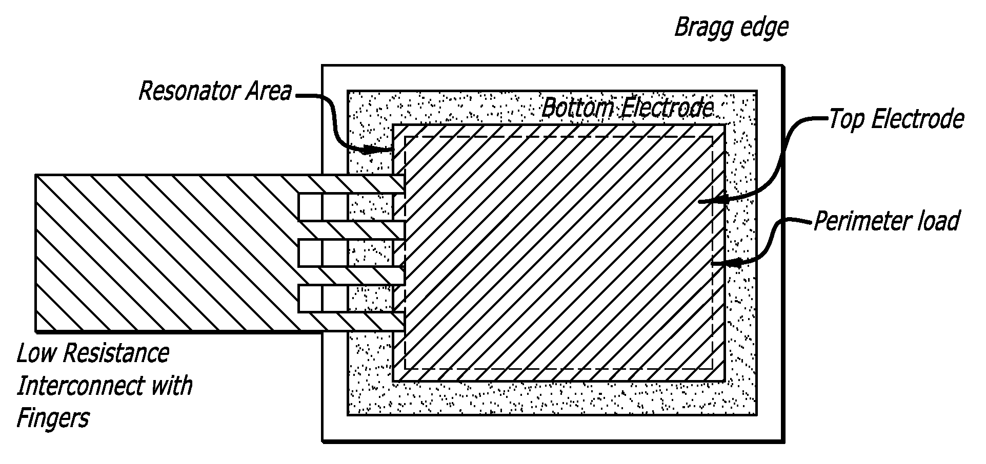
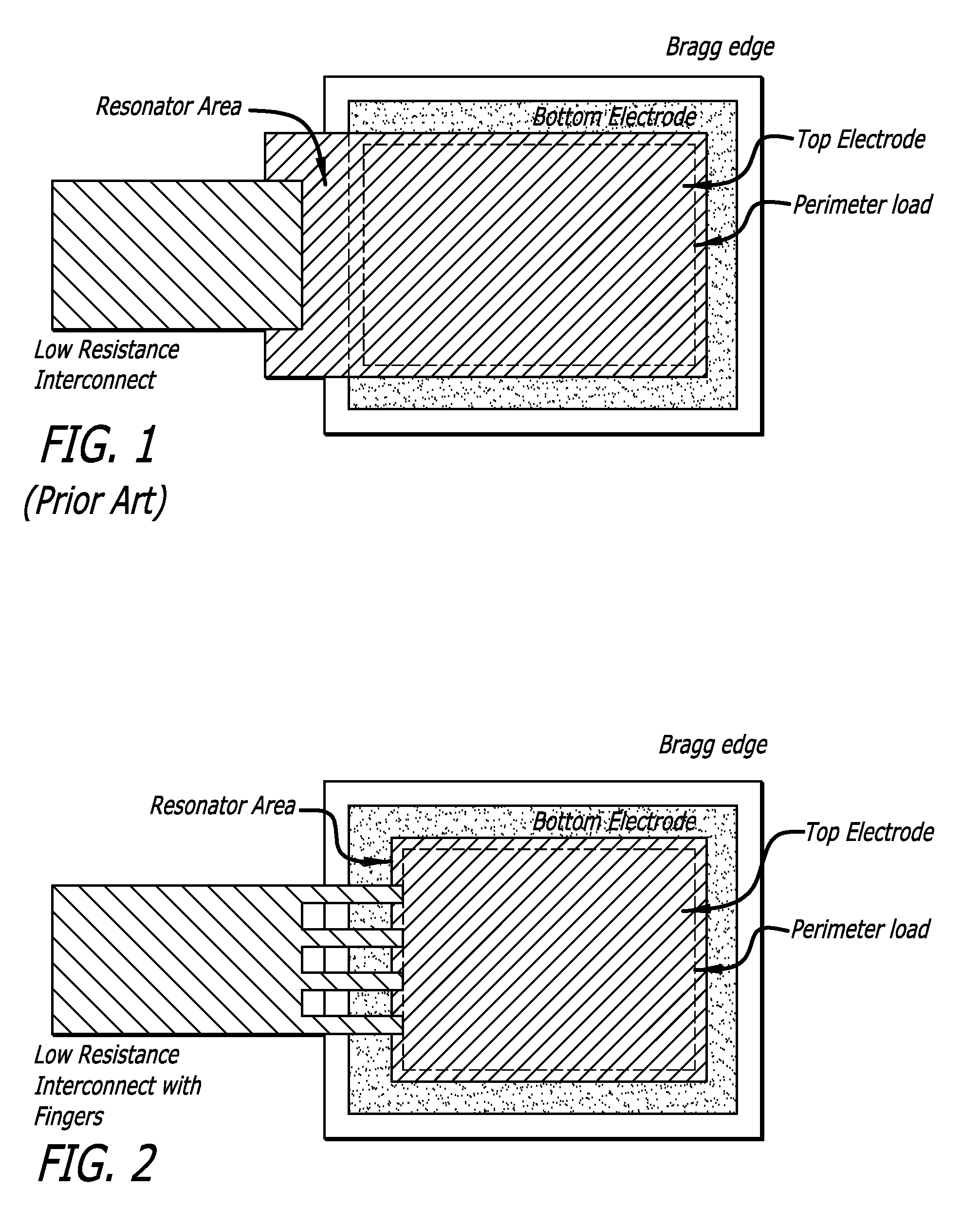
[0016]The present invention pertains to how to make electrical contact to a resonator with minimal added losses or other impact on the resonator characteristics. In particular, electrical connection must be made to the top electrode of the resonator. Any physical contact to the top electrode will have associated acoustic losses (e.g. losses from parasitic or spurious resonances caused by non-uniform loading). The problem is how to contact the top electrode of a resonator with minimum electrical resistance, minimal acoustic loading at the top electrode edge, and maximize conduction spread (i.e. signal feed). Acoustic problems arise from non-symmetry of the resonator at the electrical contact area, from piezoelectric defects and poor crystal alignment at or near the bottom electrode edge, and from excessive loading or non-uniform perimeter loading. Extrinsic conduction problems arise from high resistance interconnect materials and from excessive width of the interconnect feed. In the ...


PUM


Abstract

Methods of contacting the top layer in a BAW device by depositing a metal layer over the BAW device, patterning the metal layer so that the metal layer extends over and contacts the top electrode layer of the BAW device only at a plurality of spaced apart locations adjacent the periphery of the active resonator area, and has a common region laterally displaced from the top and bottom electrodes and electrically interconnecting the parts of the metal layer extending over and contacting the top electrode of the BAW device at the plurality of spaced apart locations.

Description

BACKGROUND OF THE INVENTION[0001]1. Field of the Invention[0002]The present invention relates to the field of piezoelectric resonators whose primary application is for signal filtering and reference oscillators.[0003]2. Prior Art[0004]The present invention pertains to piezoelectric resonators whose primary application is for signal filtering and reference oscillators. These resonators are commonly referred to as BAW (bulk acoustic wave resonators). Other acronyms for the same or similar devices include FBAR (film bulk acoustic resonators) or SMR (solidly mounted resonators), or TFR (thin film resonators) or SCF (stacked crystal filters).[0005]The resonators must be as efficient as possible in terms of energy losses. These devices are not new and are well documented in the literature.[0006]Standard IC fabrication methods are used for the basic manufacturing sequences, including depositions, photolithography, and etch processes. MEMS techniques may also be employed for packaging and r...

Claims


Application Information

Patent Timeline
IPC IPC(8): H01L41/047H01L41/08
CPCH03H9/132
Inventor WALL, RALPH N.BOUCHE, GUILLAUMEGODSHALK, EDWARD MARTINLUTZ, RICK D.SUNDBERG, GARTH
Owner QORVO US INC
Why Eureka
Try Eureka