Optical device and manufacturing method thereof

a manufacturing method and optical device technology, applied in the field of optical devices, can solve the problems of increased manufacturing cost, high glass plate cost, and inability of optical devices to receive or emit blue-violet laser ligh

Inactive Publication Date: 2009-04-02
PANASONIC CORP
View PDF7 Cites 35 Cited by
  • Summary
  • Abstract
  • Description
  • Claims
  • Application Information

AI Technical Summary

Benefits of technology

[0016]The bottom recess may have a tapered shape having a smaller opening area on a bottom-surface side.

Problems solved by technology

However, such optical devices cannot be used to receive or emit blue-violet laser light having a wavelength as short as 405 nanometers (nm) because transparent resin discolors with time and the transmittance changes.
However, such a glass plate is very expensive, and the manufacturing cost is increased.
In manufacturing of the optical function element module described in Japanese Laid-Open Patent Publication No. 2006-186288, it is difficult to control dropping of the liquid sealing resin so as to form a desired amount of sealing resin with a desired shape only within a desired range.
This results in reduction in yield.
However, this makes it impossible to achieve size reduction which is one of the objects of Japanese Laid-Open Publication No. 2006-186288.

Method used


Image

  • Optical device and manufacturing method thereof
  • Optical device and manufacturing method thereof
  • Optical device and manufacturing method thereof

Examples


first embodiment

Structure of an Optical Device

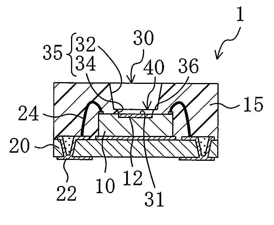
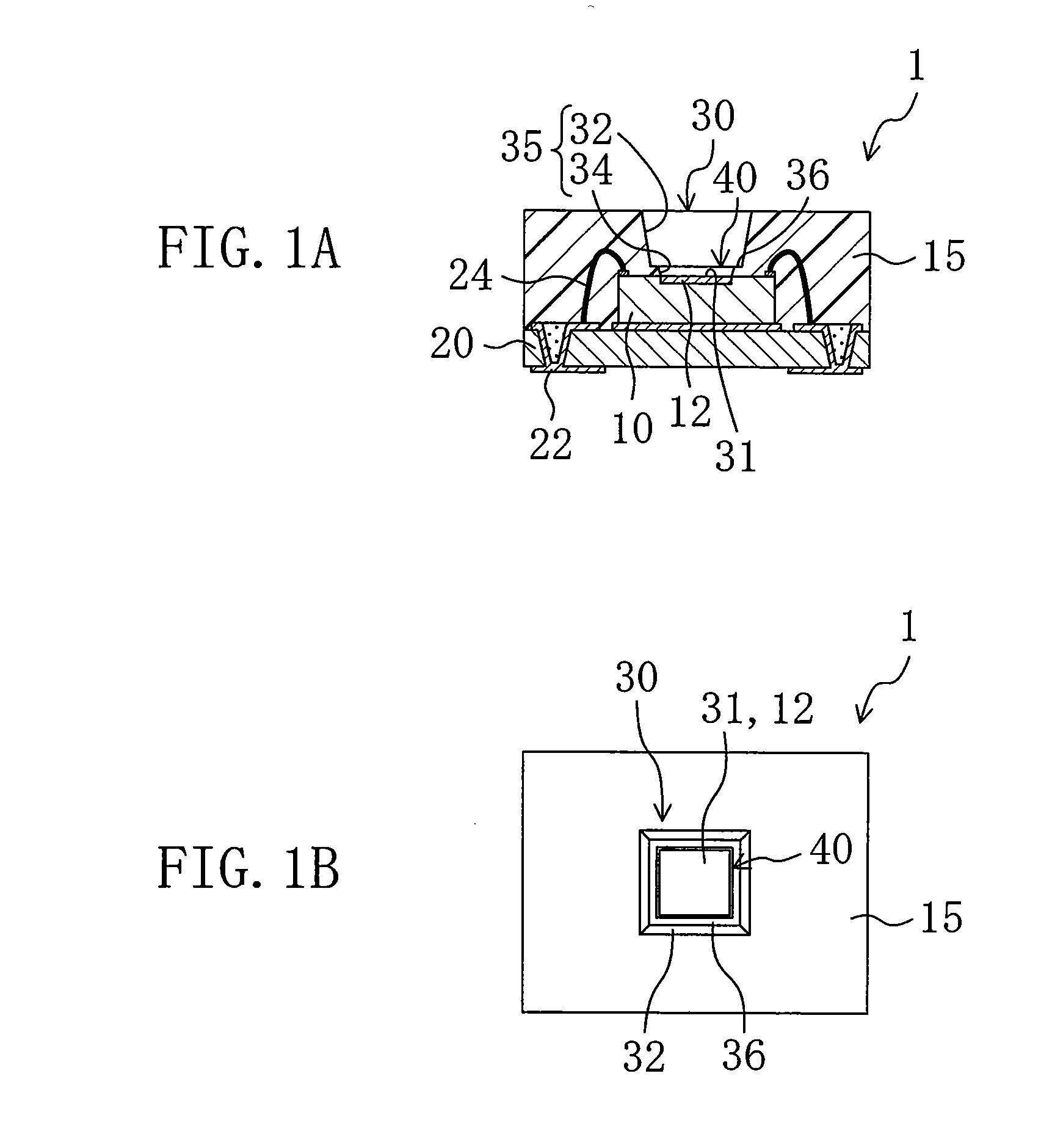
[0030]FIG. 1A is a cross-sectional view of an optical device (light-receiving device) 1 according to a first embodiment of the invention. FIG. 1B is a top view of the optical device 1. The optical device 1 is formed by resin-sealing an optical element (light-receiving element) 10 mounted on a wiring board 20 with a sealing resin 15 so as to expose an optical function region (light-receiving portion) 12.

[0031]The optical element 10 that is a semiconductor element has a rectangular flat plate shape. The optical function region 12 is formed in the center of one surface of the optical element 10. Electrode pads are provided on the periphery of this surface of the optical element 10. The optical element 10 is fixed to the wiring board 20 by mounting the other surface of the optical element 10 (the surface on which the optical function region 12 is not formed) on the wiring board 20. In other words, the optical element 10 is mounted on the wiring board 20 and...

second embodiment

[0053]In an optical device 2 of a second embodiment shown in FIGS. 5A and 5B, an optical element 11 has three optical function regions 14, 16, and 18. The shape of a recess 30a is therefore partially different from that of the recess 30 of the first embodiment. However, components such as the wiring board 20 and the wires 24 are the same as those of the first embodiment. Therefore, only the differences from the first embodiment will be described below and description of the same portions will be omitted.

[0054]In the optical device 2 of this embodiment, three light-receiving portions (optical function regions 14, 16, and 18) having different functions are arranged next to each other. In this embodiment, the light-receiving portion located in the middle is a main light-receiving portion. The light-receiving portions located on both sides have a function to confirm if the main light-receiving portion is properly receiving light or not. In other words, if a predetermined amount of light...

third embodiment

[0058]In an optical device 3 of a third embodiment shown in FIG. 6, the shape of a recess 30b is partially different from that of the recess 30 of the first embodiment. However, components such as the wiring board 20 and the wires 24 are the same as those of the first embodiment. Therefore, only the differences from the first embodiment will be described below and description of the same portions will be omitted.

[0059]In the optical device 3 of this embodiment, a second side surface 32 of a side surface 35b is the same as the second side surface 32 of the first embodiment, but a first side surface 34b of the side surface 35b is different from the first side surface 34 of the first embodiment. Unlike the first side surface 34 of the first embodiment, a bottom recess 42 formed by the first side surface 34b and the bottom surface 31b has a tapered shape having a larger opening area at the bottom. Such a bottom recess 42 can be easily formed by using a negative resist as the resist 17 p...


PUM

PropertyMeasurementUnit
optical functionaaaaaaaaaa
depthaaaaaaaaaa
areaaaaaaaaaaa

Abstract

An optical element mounted on a wiring board is sealed by a sealing resin except an optical function region. Wires connecting the wiring board with the optical element are also sealed by the sealing resin. The optical function region is exposed as a bottom surface of a recess whose side surface is formed by the sealing resin. The recess has a two-level structure of a bottom recess and a portion located over the bottom recess. A stepped portion extends from an upper end of a first side surface of the bottom recess to a lower end of a second side surface of the bottom recess.

Description

BACKGROUND OF THE INVENTION[0001]1. Field of the Invention[0002]The invention relates to an optical device and a manufacturing method thereof. More particularly, the invention relates to an optical device including an optical element and a wiring board having the optical element mounted thereon, in which an electrically connected portion of the optical element and the wiring board is resin-sealed, and a manufacturing method of the optical device.[0003]2. Related Art[0004]Optical devices having an optical semiconductor device, such as a solid state imaging element and an LED (Light Emitting Diode), mounted on a wiring board have been known in the art. An example of such an optical device has a hollow package structure in which a light-transmitting substrate is provided over an optical function surface in order to protect the optical function surface (for example, see Japanese Laid-Open Patent Publication No. 2003-332542). In another example of such an optical device, a transparent re...

Claims


Application Information

Patent Timeline
Patent Type & Authority Applications(United States)
IPC IPC(8): H05K7/00B29D11/00H01L33/56H01L33/62
CPCH01L27/14618H01L31/0203H01L2224/97H01L2924/01029H01L2924/1815H01L2224/73265H01L2224/48227H01L2224/32225H01L24/97H01L2924/12041H01L33/60H01L33/486H01L2224/48091H01L2924/00014H01L2924/00H01L2924/00012H01L2224/92247H01L24/73
Inventor MINAMIO, MASANORITANIGUCHI, MASAKIISHIDA, HIROYUKIYOSHIKAWA, NORIYUKI
Owner PANASONIC CORP
Why Eureka
Try Eureka