
Image Forming Device

a technology of forming device and image, which is applied in the direction of inking apparatus, electrographic process, instruments, etc., can solve the problems of user preparation and difficulty in cleaning the exposure surface of the user

Inactive Publication Date: 2009-04-02
BROTHER KOGYO KK
View PDF2 Cites 25 Cited by
  • Summary
  • Abstract
  • Description
  • Claims
  • Application Information

AI Technical Summary

Benefits of technology

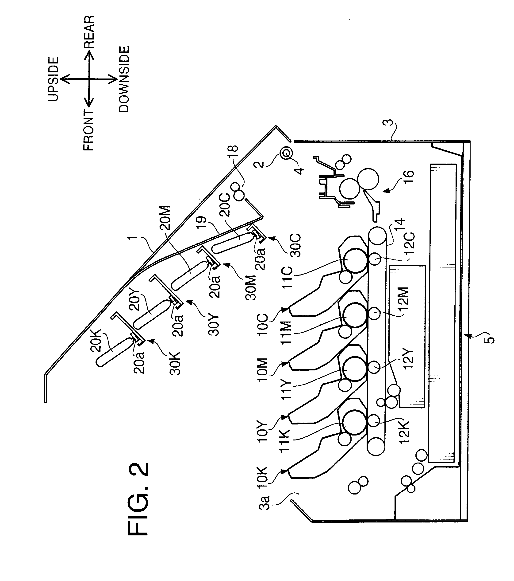
[0009]In the above known image forming device with the LED heads 111 held by the stacker cover 107, a mechanism in which the LED heads 111 are turned in conjunction with opening and closing of the stacker cover 107 may be applied. In this case, the LED heads 111 are disposed in exposure positions to expose the circumferential surface of the photoconductive bodies 103a when the stacker cover 107 is closed. Further, the LED heads 111 are disposed in evacuation positions where the LED heads 111 are substantially parallel to the stacker cover 107, when the stacker cover 107 is opened. Thereby, it is possible to prevent the LED heads 111 from disturbing replacement of the drum units 103.
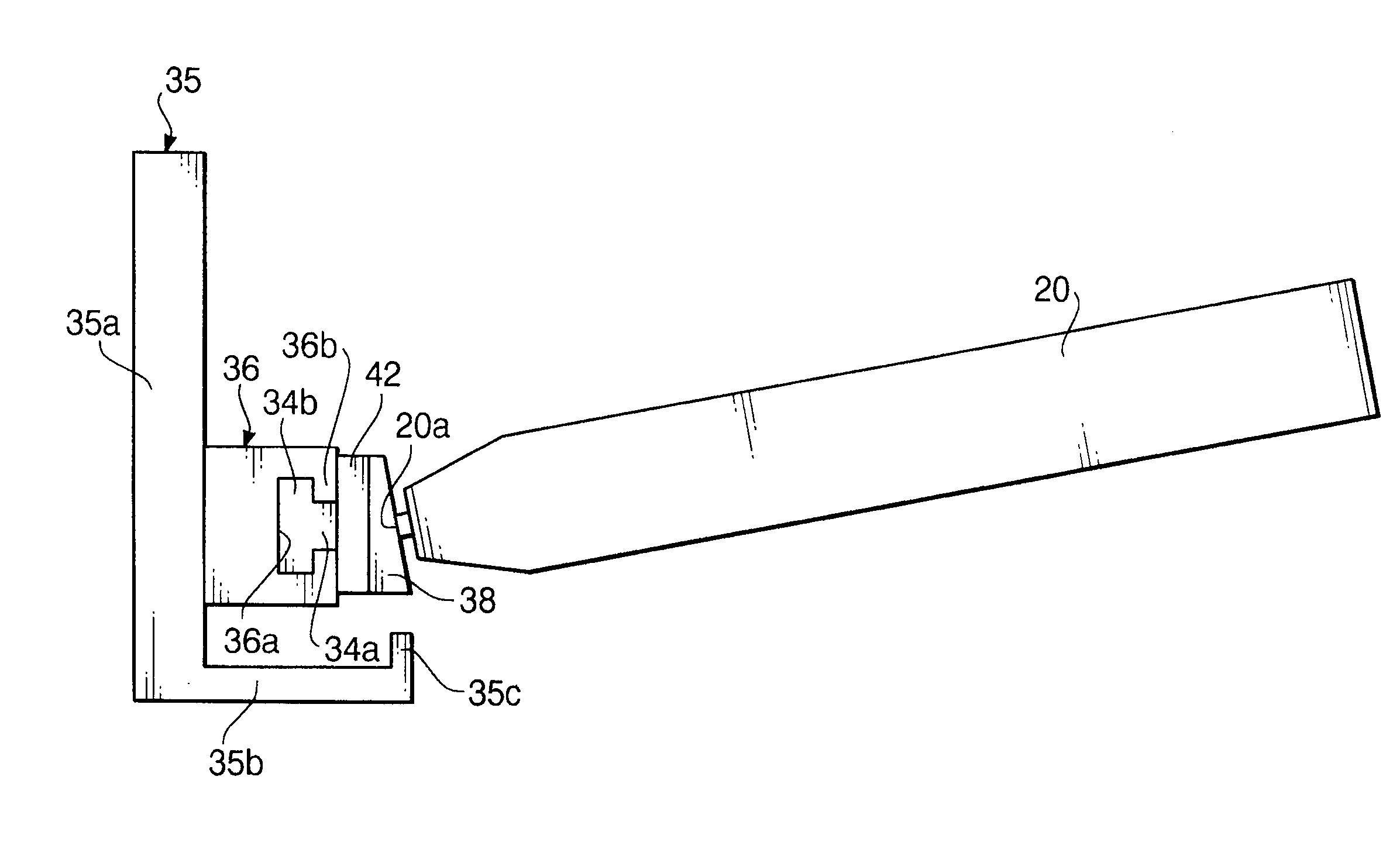
[0012]Aspects of the present invention is advantageous to provide one or more improved image forming devices that make it possible to easily clean an exposure surface of an exposure unit thereof.
[0015]In some aspects, it is possible to easily clean the exposure surface of the exposure unit provided to the second device body with the cleaning unit. Thus, it is possible to prevent formation of an uneven image due to the exposure surface contaminated with toner.

Problems solved by technology

However, the above image forming device with the LED heads 111 held by the stacker cover 107 is not provided with any cleaning member for cleaning the exposure surfaces.
Therefore, there is a problem that a user has to prepare for a cleaning member and clean the exposure surfaces.
Hence, there is another problem that it is difficult for the user to clean the exposure surfaces.

Method used


Image

  • Image Forming Device
  • Image Forming Device
  • Image Forming Device

Examples


Embodiment Construction

[0026]It is noted that various connections are set forth between elements in the following description. It is noted that these connections in general and, unless specified otherwise, may be direct or indirect and that this specification is not intended to be limiting in this respect.

[0027]Hereinafter, embodiments according to aspects of the present invention will be described with reference to the accompany drawings.

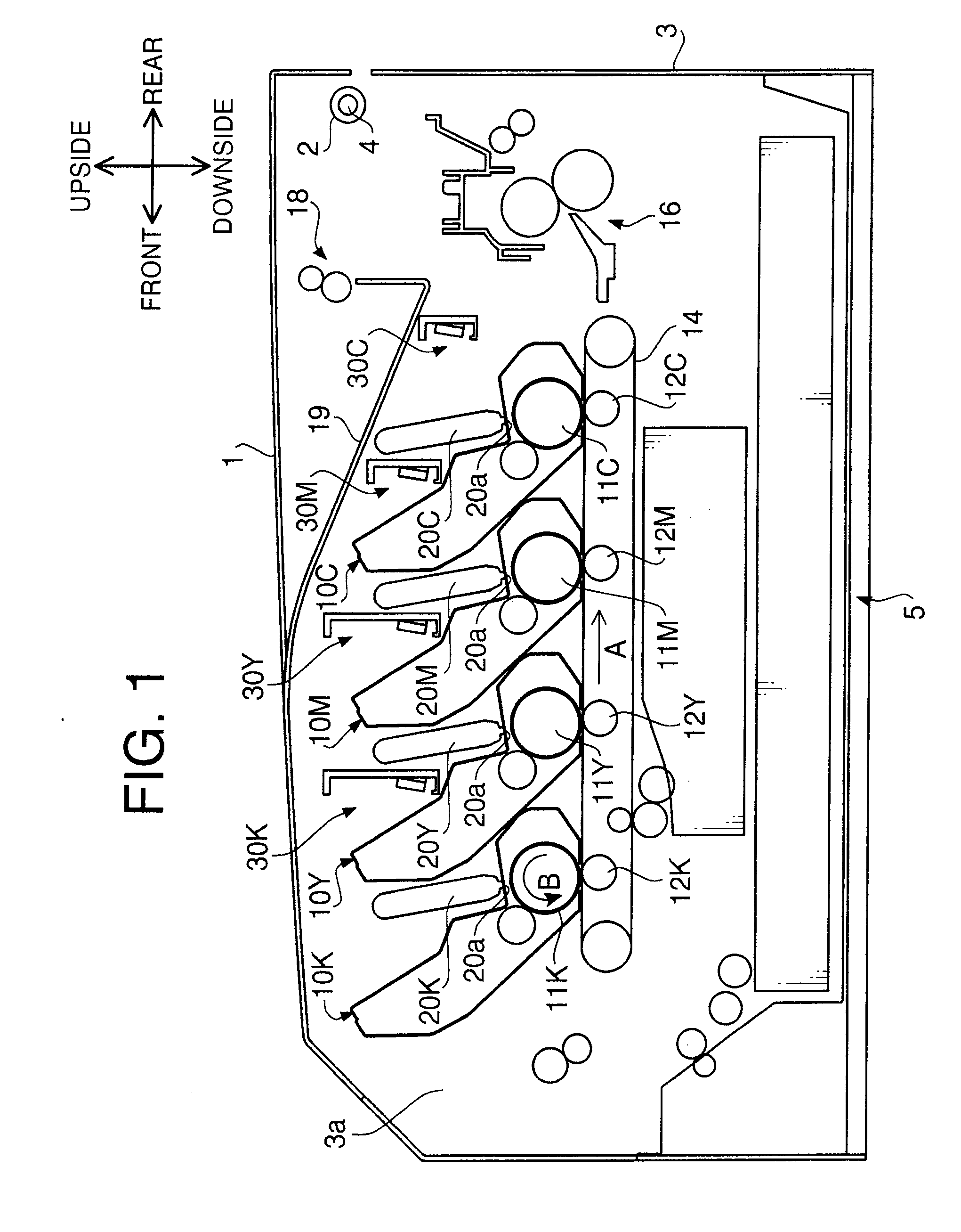
[0028]FIG. 1 is a cross-sectional view schematically showing an entire configuration of an LED printer 5 in a first embodiment according to aspects of the present invention. In the LED printer 5 shown in FIG. 1, a left side, a right side, a back side, and a front side on the figure are defined as a front side, a rear side, a left side, and a right side, respectively.

[0029]In FIG. 1, an upper case 1 is supported, rotatably with respect to a mechanical unit 3, by a rotational shaft hole 2 provided at a rear side of the upper case 1 and a rotational shaft 4 provided at a re...


PUM


Abstract

An image forming device includes a first device body, a second device body attached to the first device body, a photoconductive body provided in the first device body, an exposure unit provided to the second device body, the exposure unit having an exposure surface that exposes the photoconductive body and forms a latent image on the photoconductive body, the exposure unit being movable between an exposure position and an evacuation position, and a cleaning unit cleaning the exposure surface of the exposure unit. The cleaning unit includes a cleaning member cleaning the exposure surface, a supporting member supporting the cleaning member, and a guide member movably guiding the supporting member. The exposure unit is disposed such that the exposure surface is cleaned by the cleaning unit when the exposure unit is moved to the evacuation position.

Description

CROSS-REFERENCE TO RELATED APPLICATIONS[0001]This application claims priority under 35 U.S.C. §119 from Japanese Patent Application No. 2007-253921 filed on Sep. 28, 2007. The entire subject matter of the application is incorporated herein by reference.BACKGROUND [0002]1. Technical Field[0003]The following description relates to one or more image forming devices such as an electrophotographic copy machine and a printer.[0004]2. Related Art[0005]In an image forming device such as an electrophotographic copy machine and a printer, a laser scanning method and an LED exposure method have been put into practical use as an image writing method (i.e., an exposure method). The LED exposure method is a method in which light emitted by a light emitting unit with a plurality of light emitting elements linearly aligned is directed onto a surface of a photoconductive body with an imaging system and a latent image is formed on the surface of the photoconductive body.[0006]FIG. 10 schematically sh...

Claims


Application Information

Patent Timeline
IPC IPC(8): G03G21/00
CPCG03G15/011G03G2215/0141G03G2215/0409G03G15/04054G03G2221/1687G03G21/1666G03G2221/1636
Inventor TERAO, AKIRAAKATSUKA, YASUNORI
Owner BROTHER KOGYO KK
Learn More