Solid state light emitting device

a light-emitting device and solid-state technology, applied in the direction of semiconductor devices, semiconductor/solid-state device details, electrical devices, etc., can solve the problem of degrading the luminous efficiency of leds

Inactive Publication Date: 2009-04-09
FOXSEMICON INTEGRATED TECH INC
View PDF10 Cites 32 Cited by
  • Summary
  • Abstract
  • Description
  • Claims
  • Application Information

AI Technical Summary

Benefits of technology

[0006]The present invention provides a solid state light emitting device endowed with additional functions without having to degrade the luminous efficiency. The solid state light emitting device includes a laminated substrate structure, an LED chip, a transparent capsulation material and an electric component. The laminated substrate structure includes a first substrate and a second substrate attached to each other by a sintering pr

Problems solved by technology

However, the black outer surface would absorb some of light emitted from a LED chip arranged on the surface of

Method used


Image

  • Solid state light emitting device
  • Solid state light emitting device
  • Solid state light emitting device

Examples


Embodiment Construction

[0017]Reference will now be made to the drawing figures to describe the preferred embodiment in detail.

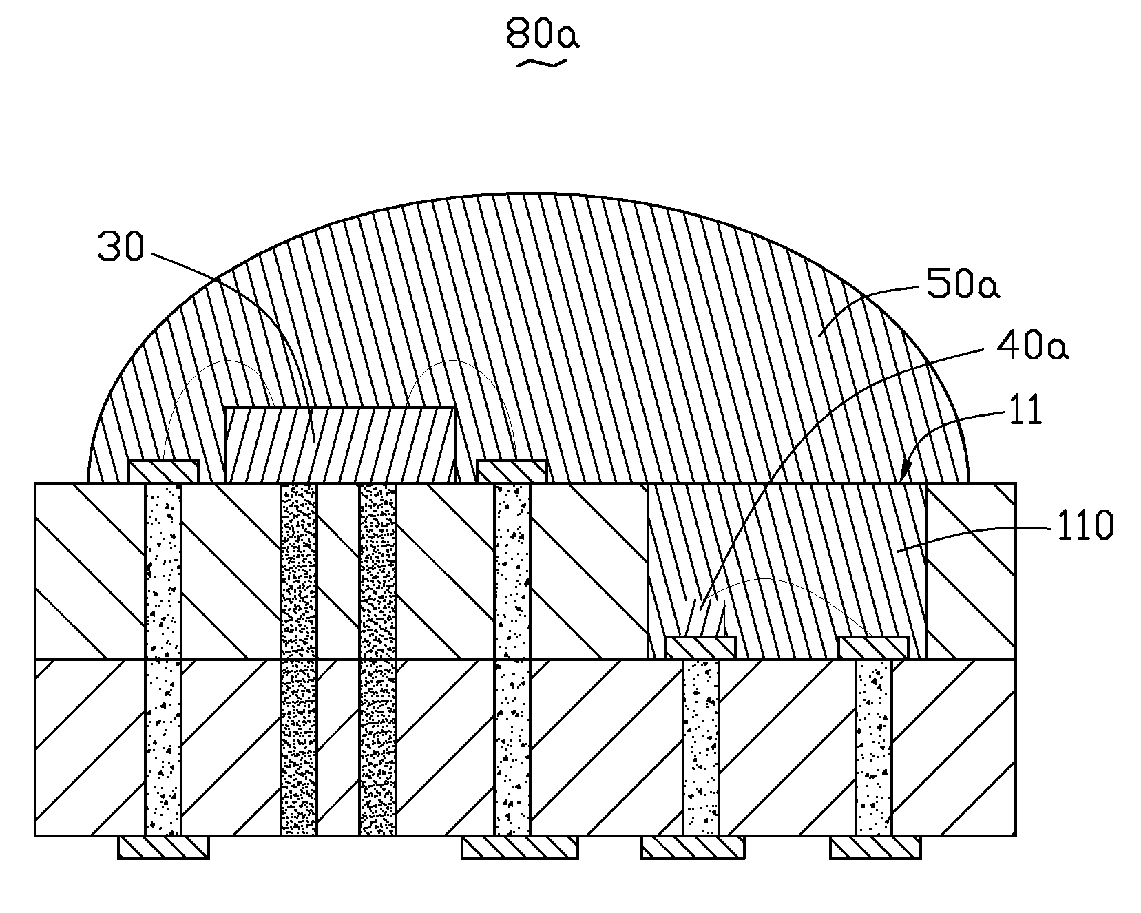
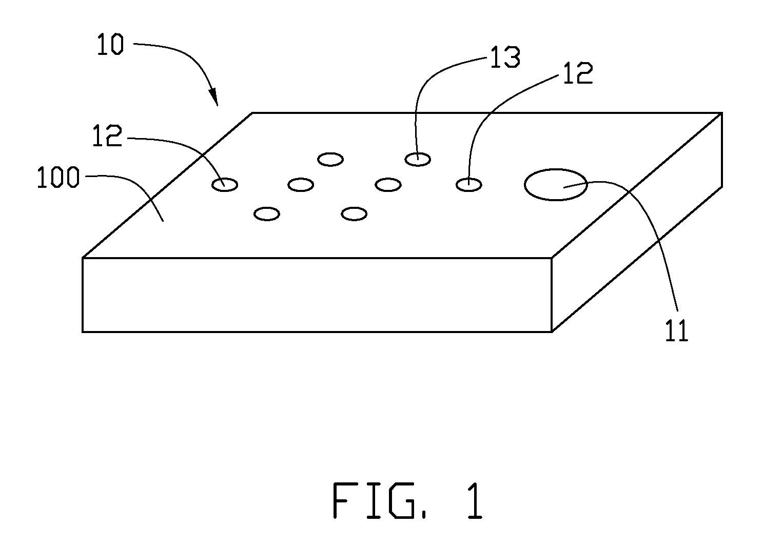
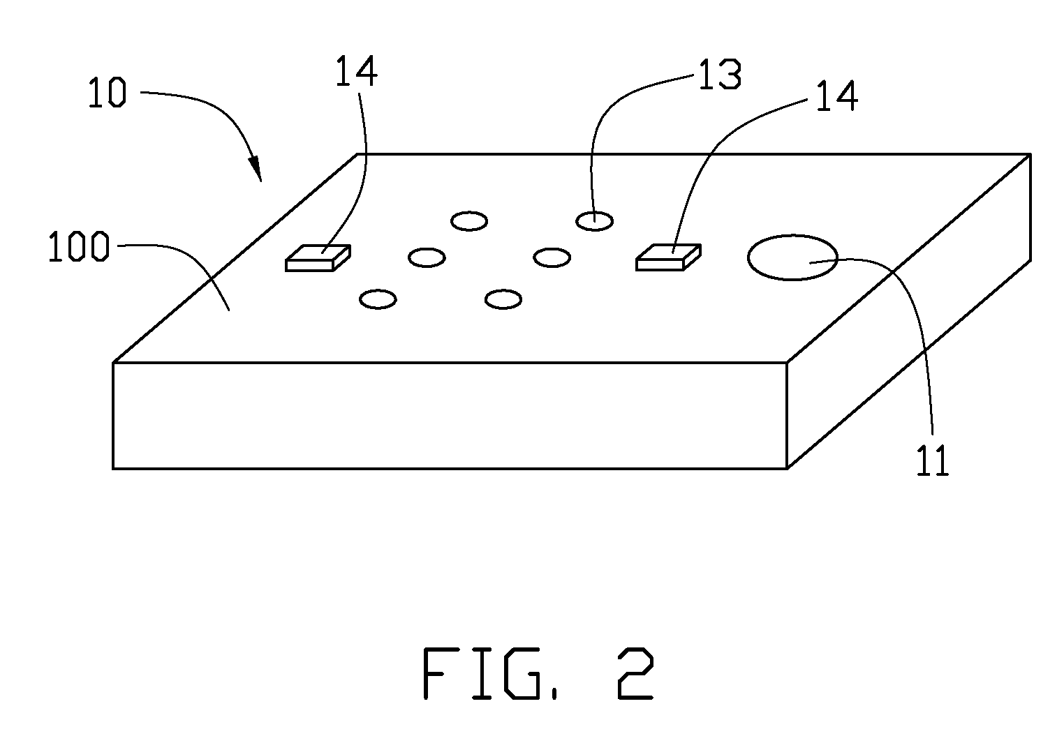
[0018]The present embodiment provides a solid state light emitting device, such as a LED (light emitting diode), which is endowed with additional functions without having to degrade the illumination efficiency. The solid state light emitting device includes a laminated substrate structure 120 which is manufactured by the flowing steps: 1) providing a first substrate 10 which includes a first surface 100 (mounting surface of the first substrate 10), the first surface 100 of the first substrate 10 defining a receiving hole 11 configured for receiving an electric component therein (this step is shown in FIG. 1); 2) providing a second substrate 20 (this step is shown in FIG. 3); 3) stacking the first and the second substrates 10, 20 together; 4) co-sintering the first and the second substrates 10, 20 so that the first substrate 10 is fired into a single piece (this step is shown in FIG...


PUM


Abstract

A solid state light emitting device includes a laminated substrate structure (120), an LED chip (30), a transparent capsulation material (50) and an electric component (40). The laminated substrate structure includes a first substrate (10) and a second substrate (20) attached to each other by a sintering process. The first substrate has a mounting surface (100) and a receiving through hole (11) defined in the mounting surface thereof. The LED chip is mounted on the mounting surface of the first substrate. The transparent capsulation material envelops the LED chip therein. The electric component is received in the receiving hole and mounted on the second substrate. The electric component is located below the mounting surface of the first substrate.

Description

BACKGROUND[0001]1. Technical Field[0002]The present invention generally relates to solid state light emitting devices and method for manufacturing substrates thereof.[0003]2. Description of Related Art[0004]LEDs (light emitting diodes) each is a type of solid state light emitting device and are widely used in daily life, such as in illumination devices or non-emissive display devices, due to its high brightness, long life-span, and wide color gamut. The researches of LEDs are disclosed in a paper on IEEE Transactions on Electron Devices, entitled “Design and fabrication of AlGaInP LED array with integrated GaAs decode circuits”, published by Rong-Ting Huang et al., in 1998, the disclosure of which is incorporated herein by reference.[0005]In ordinary use, an electric component is usually enveloped in the LED for improving the reliability and practicability of the LED. For instance, mounting a zener diode on a surface of a substrate of the LED for increasing electrostatic prevention ...

Claims


Application Information

Patent Timeline
IPC IPC(8): H01L33/00H01L33/48
CPCH01L25/167H01L33/486H01L2924/09701H01L2224/45144H01L2924/12032H01L2224/48227H01L2224/48091H01L2924/00014H01L2924/00
Inventor WANG, CHUN-WEIHSU, HUNG-KUANGJIANG, WEN-JANG
Owner FOXSEMICON INTEGRATED TECH INC
Why Eureka
Try Eureka