Semiconductor memory device including double spacers on sidewall of flating gate, electronic device including the same

Active Publication Date: 2009-04-16
SAMSUNG ELECTRONICS CO LTD
View PDF0 Cites 2 Cited by
  • Summary
  • Abstract
  • Description
  • Claims
  • Application Information

AI Technical Summary

Benefits of technology

[0007]Embodiments of the present invention can be generally characterized as capable of providing a semiconductor memory device such as a nonvolatile memory device that can remove a read error. Embodiments o

Problems solved by technology

Volatile memory devices lose stored data in the event of power interruption, whereas nonvolatile memory devices retain stored data even if p

Method used


Image

  • Semiconductor memory device including double spacers on sidewall of flating gate, electronic device including the same
  • Semiconductor memory device including double spacers on sidewall of flating gate, electronic device including the same
  • Semiconductor memory device including double spacers on sidewall of flating gate, electronic device including the same

Examples


Example

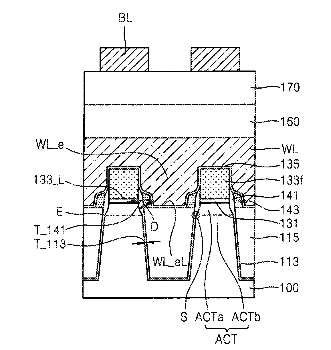
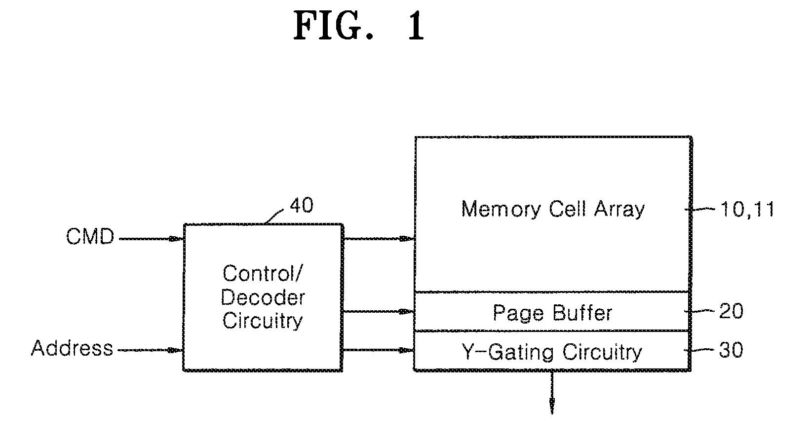
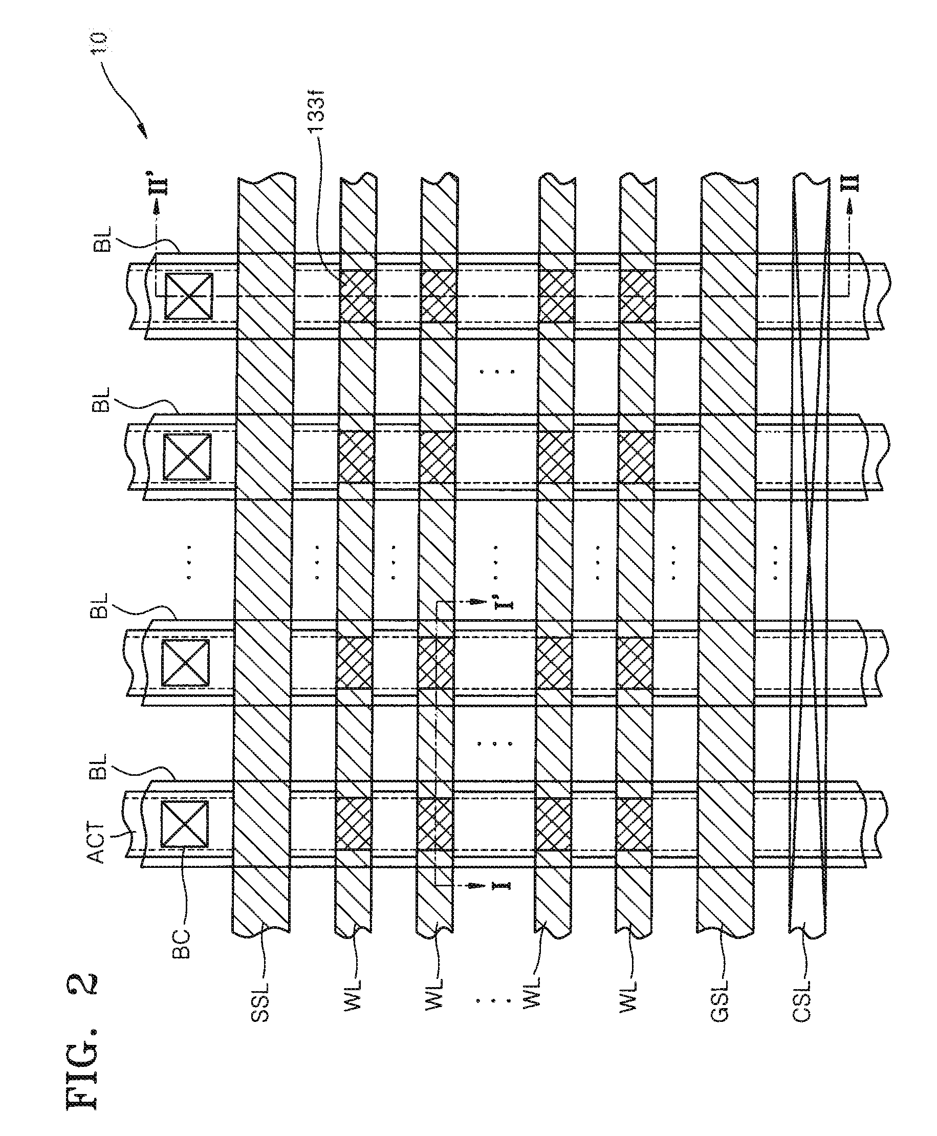
[0019]Reference will now be made in detail to the accompanying drawings, which illustrate example embodiments of the present invention. However, the example embodiments are not limited to the illustrations provided by the drawings and detailed description thereof. Rather, the drawings and accompanying detailed description are introduced to provide easy and complete understanding of the scope and spirit of example embodiments. In the drawings, the thicknesses of layers and regions are exaggerated for clarity.

[0020]It will be understood that when an element, such as a layer, a region, or a substrate, is referred to as being “on,”“connected to” or “coupled to” another element, it may be directly on, connected or coupled to the other element or intervening elements may be present. In contrast, when an element is referred to as being “directly on,”“directly connected to” or “directly coupled to” another element or layer, there are no intervening elements or layers present. Like reference...


PUM


Abstract

A semiconductor memory device includes a device isolation layer formed in a semiconductor substrate to define a plurality of active regions. Floating gates are disposed on the active regions. A control gate line overlaps top surfaces of the floating gates and crosses over the active regions. The control gate line has an extending portion disposed in a gap between adjacent floating gates and overlapping sidewalls of the adjacent floating gates. First spacers are disposed on the sidewalls of the adjacent floating gates. Each of the first spacers extends along a sidewall of the active region and along a sidewall of the device isolation layer. Second spacers are disposed between outer sidewalls of the first spacers and the extending portion and are disposed above the device isolation layer. An electronic device including a semiconductor memory device and a method of fabricating a semiconductor memory device are also disclosed.

Description

CROSS-REFERENCE TO RELATED PATENT APPLICATION[0001]This application claims the benefit of foreign priority to Korean Patent Application No. 10-2007-0103708, filed on Oct. 15, 2007, the disclosure of which is incorporated herein in its entirety by reference.BACKGROUND[0002]1. Field of Invention[0003]Embodiments of the present invention relate generally to semiconductor memory devices, and more particularly, to a semiconductor memory device such as a nonvolatile memory device.[0004]2. Description of the Related Art[0005]Semiconductor memory devices, which store data, are generally classified as volatile memory devices or nonvolatile memory devices. Volatile memory devices lose stored data in the event of power interruption, whereas nonvolatile memory devices retain stored data even if power is interrupted.[0006]A flash memory device is a type of nonvolatile memory device that is capable of electrically writing and erasing data, and is suitable for high density and high capacitance. A ...

Claims


Application Information

Patent Timeline
IPC IPC(8): H01L27/088
CPCH01L27/115H01L27/11524H01L27/11521H10B69/00H10B41/35H10B41/30H01L21/28141H01L21/31051H01L21/76838
Inventor LIM, JOON-SUNGPARK, JONG-HOBACK, HYUN-CHULLEE, SUNG-HUN
Owner SAMSUNG ELECTRONICS CO LTD
Why Eureka
Try Eureka