Signal processing device for solid-state imaging device, imaging apparatus having the signal processing device, signal processing method, and program

a solid-state imaging and signal processing technology, applied in the direction of instruments, television systems, television system scanning details, etc., can solve the problem of inability to properly correct inter-pixel color mixing

Inactive Publication Date: 2009-04-16
SONY CORP
View PDF5 Cites 16 Cited by
  • Summary
  • Abstract
  • Description
  • Claims
  • Application Information

AI Technical Summary

Benefits of technology

[0026]According to the embodiments of the invention, it is possible to provide a signal processing device for a solid-state imaging device, an imaging apparatus having such a signal processing device, a signal processing method, and a program which allow inter-pixel color mixing to be corrected even when color mixing ratios are two-dimensionally distributed in a pixel array surface.
[0027]According to the embodiments of the invention, it is possible to provide a signal processing device for a solid-state imaging device, an imaging apparatus having such a signal processing device, a signal processing method, and a program which allow a signal for a pixel of interest to be properly processed even when parameters are two-dimensionally distributed in a pixel array surface.

Problems solved by technology

Specifically, since color mixing ratios are two-dimensionally distributed in the pixel array surface, a problem arises in that inter-pixel color mixing cannot be properly corrected by using correction parameters which are uniform in the pixel array surface as done in the related art.

Method used


Image

  • Signal processing device for solid-state imaging device, imaging apparatus having the signal processing device, signal processing method, and program
  • Signal processing device for solid-state imaging device, imaging apparatus having the signal processing device, signal processing method, and program
  • Signal processing device for solid-state imaging device, imaging apparatus having the signal processing device, signal processing method, and program

Examples


first embodiment

[0060]A signal processing device and a signal processing method for correcting color mixing according to a first embodiment of the invention will now be described. In the signal processing device and signal processing method according to the present embodiment, correction parameters are two-dimensionally distributed in a pixel array surface on which a plurality of pixels are arranged.

(Functional Configuration of Signal Processing Device)

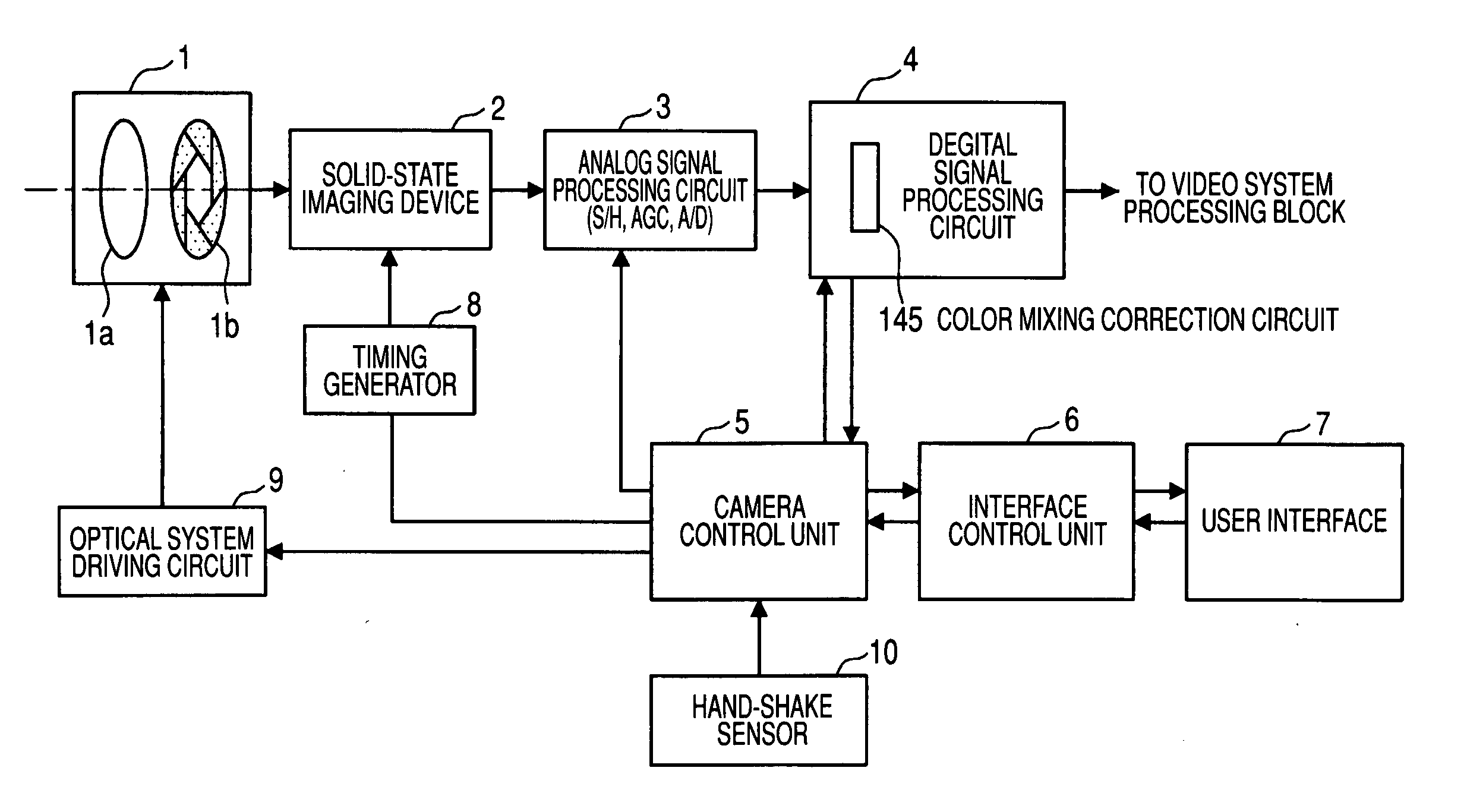
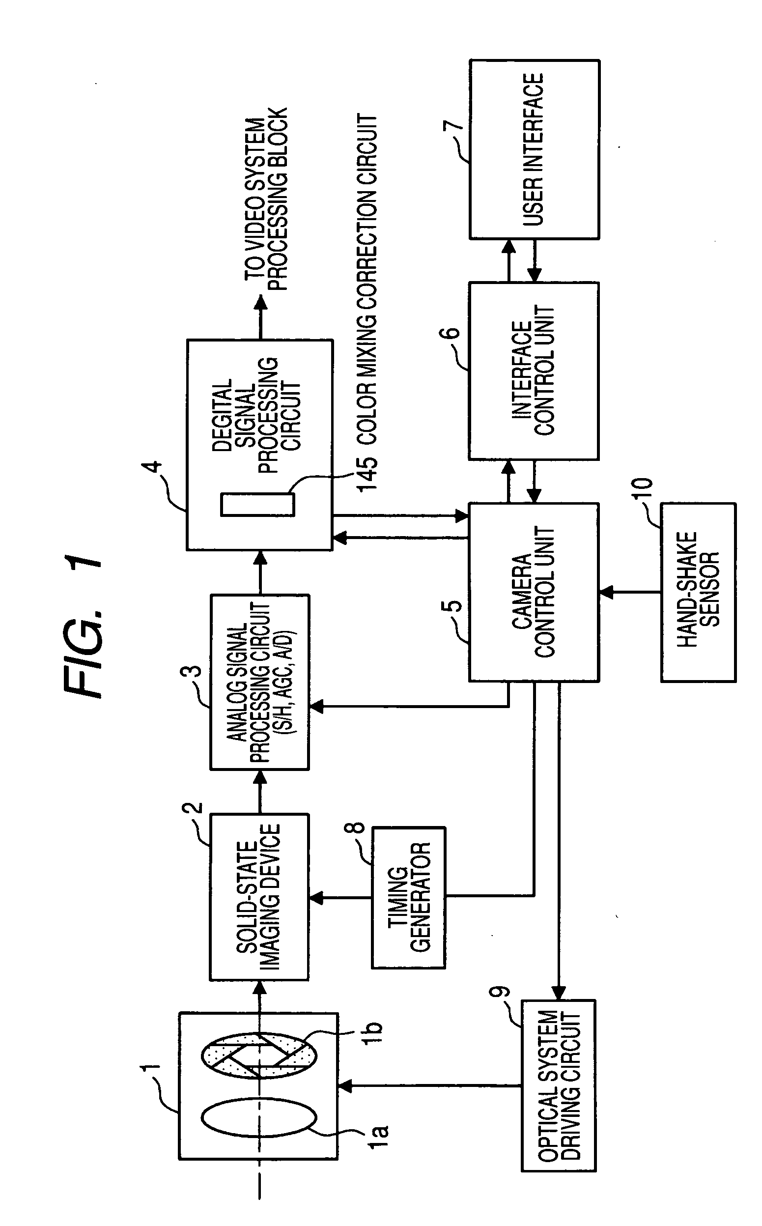
[0061]FIG. 3 is a block diagram showing a functional configuration of a color mixing correction circuit included in the signal processing device of the present embodiment.

[0062]As shown in FIG. 3, a color mixing correction circuit 145 includes a color mixing correction process unit 145a (45a) serving as a signal correction unit, and a parameter (control point) selection unit 145b and a two-dimensional parameter interpolation unit 145c serving as a parameter distribution unit. The color mixing correction process unit 145a, the parameter selection unit...

second embodiment

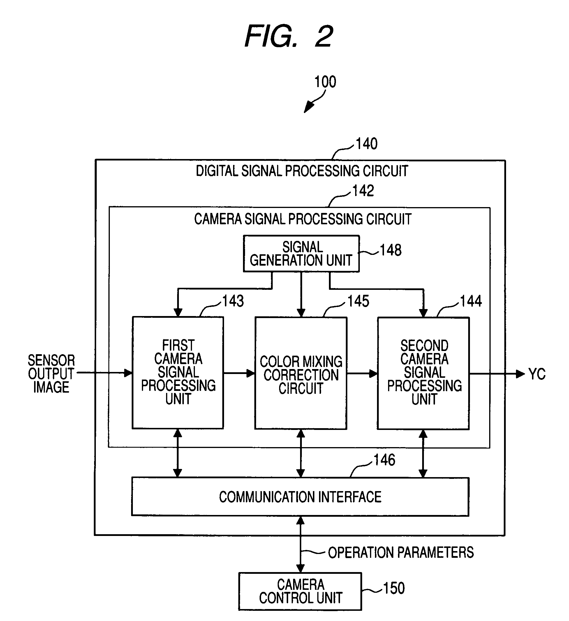
[0104]A signal processing device according to a second embodiment of the invention will now be described.

(Functional Configuration of Signal Processing Device)

[0105]FIG. 10 is a block diagram showing a functional configuration of a signal processing circuit included in the signal processing device according to the present embodiment.

[0106]Like the color mixing correction circuit 145 shown in FIG. 3, a signal processing circuit 245 includes a signal processing unit 245a and a parameter (control point) selection unit 245b and a two-dimensional parameter interpolation unit 245c serving as a parameter distribution unit. The functional configurations of the parameter selection unit 245b and the two-dimensional parameter interpolation unit 245c will not be described in detail because they are basically the same as those in the color mixing correction circuit 145 described above.

[0107]While the color mixing correction circuit 145 shown in FIG. 3 is formed as part of the signal processing d...


PUM


Abstract

A signal processing device for a solid-state imaging device correcting inter-pixel color mixing in the solid-state imaging device in which color filters having a color component constituting a primary component among luminance components and other color components are disposed on a surface of a two-dimensional array of pixels including a photoelectric conversion element is disclosed. The signal processing device includes a parameter distribution unit two-dimensionally distributing correction parameters in a pixel array surface on which a plurality of pixels are arranged and a signal correcting unit correcting a signal for a pixel of interest using each of signals for a plurality of surrounding pixels adjacent to the pixel of interest in the pixel array surface and using two-dimensionally distributed correction parameters for each of the signals.

Description

CROSS REFERENCES TO RELATED APPLICATIONS[0001]The present invention contains subject matter related to Japanese Patent Application JP 2007-269238 filed in the Japanese Patent Office on Oct. 16, 2007, the entire contents of which being incorporated herein by reference.BACKGROUND OF THE INVENTION[0002]1. Field of the Invention[0003]The present invention relates to a signal processing device for a solid-state imaging device, an imaging apparatus having the signal processing device, a signal processing method, and a program.[0004]2. Description of the Related Art[0005]A solid-state imaging device such as a CCD image sensor or CMOS image sensor has a structure in which a color filter and a light-collecting micro-lens are formed in the order listed on a surface of a pixel including a photoelectric conversion element. In such a solid-state imaging device, since a color filter is interposed between a pixel and a micro-lens, the distance between the pixel and the micro-lens is increased by t...

Claims


Application Information

Patent Timeline
Patent Type & Authority Applications(United States)
IPC IPC(8): H04N5/228H04N5/335H04N9/07
CPCG06T3/4007H04N9/045H04N5/3572H04N25/61H04N23/843
Inventor TAMAOKI, AKIHIRO
Owner SONY CORP
Why Eureka
Try Eureka