ESD protection circuit for IC with separated power domains

a protection circuit and power domain technology, applied in the direction of transistors, semiconductor devices, electrical apparatus, etc., can solve the problems of ics with separated power domains that are often damaged by esd stresses

Active Publication Date: 2009-04-16
AMAZING MICROELECTRONICS
View PDF7 Cites 32 Cited by
  • Summary
  • Abstract
  • Description
  • Claims
  • Application Information

AI Technical Summary

Benefits of technology

[0014]The advantage and spirit of the invention may be understood by the following recitations together with the appended drawings.

Problems solved by technology

ESD is one of the most important reliability issues for IC products, which must be taken into consideration during the design phase of all ICs.
In such a system-on-chip (SoC) application, the interface circuits in ICs with separated power domains are often damaged by ESD stresses.

Method used


Image

  • ESD protection circuit for IC with separated power domains
  • ESD protection circuit for IC with separated power domains
  • ESD protection circuit for IC with separated power domains

Examples


first embodiment

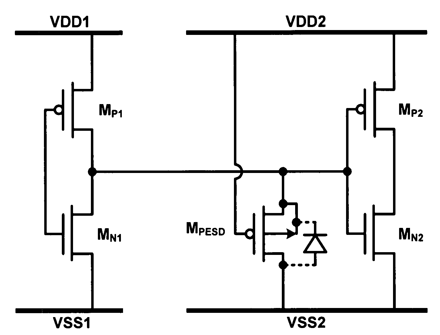
[0021]Please refer to FIG. 4, which illustrates the ESD protection circuit in the first embodiment according to the invention. In this embodiment, the ESD protection circuit includes a PMOS (MPESD). The labels VDD1 and VSS1 represent power rails in a first power domain; VDD2 and VSS2 represent power rails in a second power domain. As shown in FIG. 4, MPESD is coupled between a first circuit (MP1, MN1) in the first power domain and a second circuit (MP2, MN2) in the second power domain.

[0022]The source and body terminals of MPESD are coupled to a connection node for connecting the first circuit and the second circuit. The gate terminal of MPESD is coupled to VDD2. The drain terminal of MPESD is coupled to VSS2. In actual applications, the gate terminal of MPESD can be coupled to VDD2 via a resistor (not shown).

[0023]MPESD is used to clamp the voltage across the gate oxides of MP2 and MN2. When VDD1 is zapped by a positive ESD stress with VSS2 grounded, the ESD energy will be conducte...

second embodiment

[0031]Please refer to FIG. 8, which illustrates the ESD protection circuit in the second embodiment according to the invention. In this embodiment, the ESD protection circuit includes a detection unit 82 and a discharging unit 84. The detection unit 82 is configured in the first power domain (VDD1, VSS1). The discharging unit 84 is configured in the second power domain (VDD2, VSS2) and coupled to the detection unit 82. The discharging unit 84 is turned off during normal power operations and triggered by the detection unit 82 in an ESD event.

[0032]FIG. 9 shows an exemplary circuit of the detection unit 82 and the discharging unit 84. In this example, the detection unit 82 includes a capacitor (C), a first resistor (R1), and a PMOS (MP3). The capacitor and the first resistor are formed in series between VDD1 and VSS1. As shown in FIG. 9, the gate terminal of MP3 is coupled to the node between C and R1. The source terminal of MP3 is coupled to VDD1. The drain terminal of MP3 is coupled...


PUM


Abstract

An ESD protection circuit suitable for applying in an integrated circuit with separated power domains is provided. The circuit includes a P-type MOSFET coupled between a first circuit in a first power domain and a second circuit in a second power domain. A source terminal of the P-type MOSFET is coupled to a connection node for connecting the first circuit and the second circuit. A gate terminal of the P-type MOSFET is coupled to a positive power line of the second power domain. A drain terminal of the P-type MOSFET is coupled to a negative power line of the second power domain. A body terminal of the P-type MOSFET is also coupled to the connection node.

Description

BACKGROUND OF THE INVENTION[0001]1. Field of the Invention[0002]The present invention relates to an electrostatic discharge (ESD) protection circuit. In particular, the present invention relates to an ESD protection circuit suitable for applying in an integrated circuit (IC) with separated power domains.[0003]2. Description of the Prior Art[0004]ESD is one of the most important reliability issues for IC products, which must be taken into consideration during the design phase of all ICs. With the advance of IC fabrication technologies, more and more circuit blocks are integrated in a single chip. In such a system-on-chip (SoC) application, the interface circuits in ICs with separated power domains are often damaged by ESD stresses.[0005]A variety of ESD detection circuits for ICs with separated power domains were proposed. FIG. 1 and FIG. 2 respectively illustrate the traditional ESD protection circuits. In FIG. 1, the labels VDD1 and VSS1 represent power rails in a first power domai...

Claims


Application Information

Patent Timeline
Patent Type & Authority Applications(United States)
IPC IPC(8): H02H9/04
CPCH01L27/0266H01L2924/0002H01L2924/00
Inventor KER, MING-DUOHSIAO, YUAN-WENJIANG, RYAN HSIN-CHIN
Owner AMAZING MICROELECTRONICS
Why Eureka
Try Eureka