Image Sensor and a Method for Manufacturing Thereof

a technology of image sensor and manufacturing method, which is applied in the direction of electrical equipment, semiconductor devices, radio frequency controlled devices, etc., can solve the problems of reducing photo sensitivity and the size of a unit pixel, and achieve the effect of improving the light condensing ra

Inactive Publication Date: 2009-04-23
DONGBU HITEK CO LTD
View PDF3 Cites 9 Cited by
  • Summary
  • Abstract
  • Description
  • Claims
  • Application Information

AI Technical Summary

Benefits of technology

[0006]Embodiments of the present invention provide an image sensor and ...

Problems solved by technology

In the CMOS image sensor, as the design rule is gradually reduced...

Method used


Image

  • Image Sensor and a Method for Manufacturing Thereof
  • Image Sensor and a Method for Manufacturing Thereof
  • Image Sensor and a Method for Manufacturing Thereof

Examples


Embodiment Construction

[0010]An image sensor and a method for manufacturing thereof according to the present invention will be described with reference to the accompanying drawings.

[0011]It is to be understood that the figures and descriptions of embodiments of the present invention have been simplified to illustrate elements that are relevant for a clear understanding of the invention, while eliminating, for purposes of clarity, other elements that may be well known. Those of ordinary skill in the art will recognize that other elements may be desirable and / or required in order to implement the present invention. However, because such elements are well known in the art, and because they do not facilitate a better understanding of the present invention, a discussion of such elements is not provided herein.

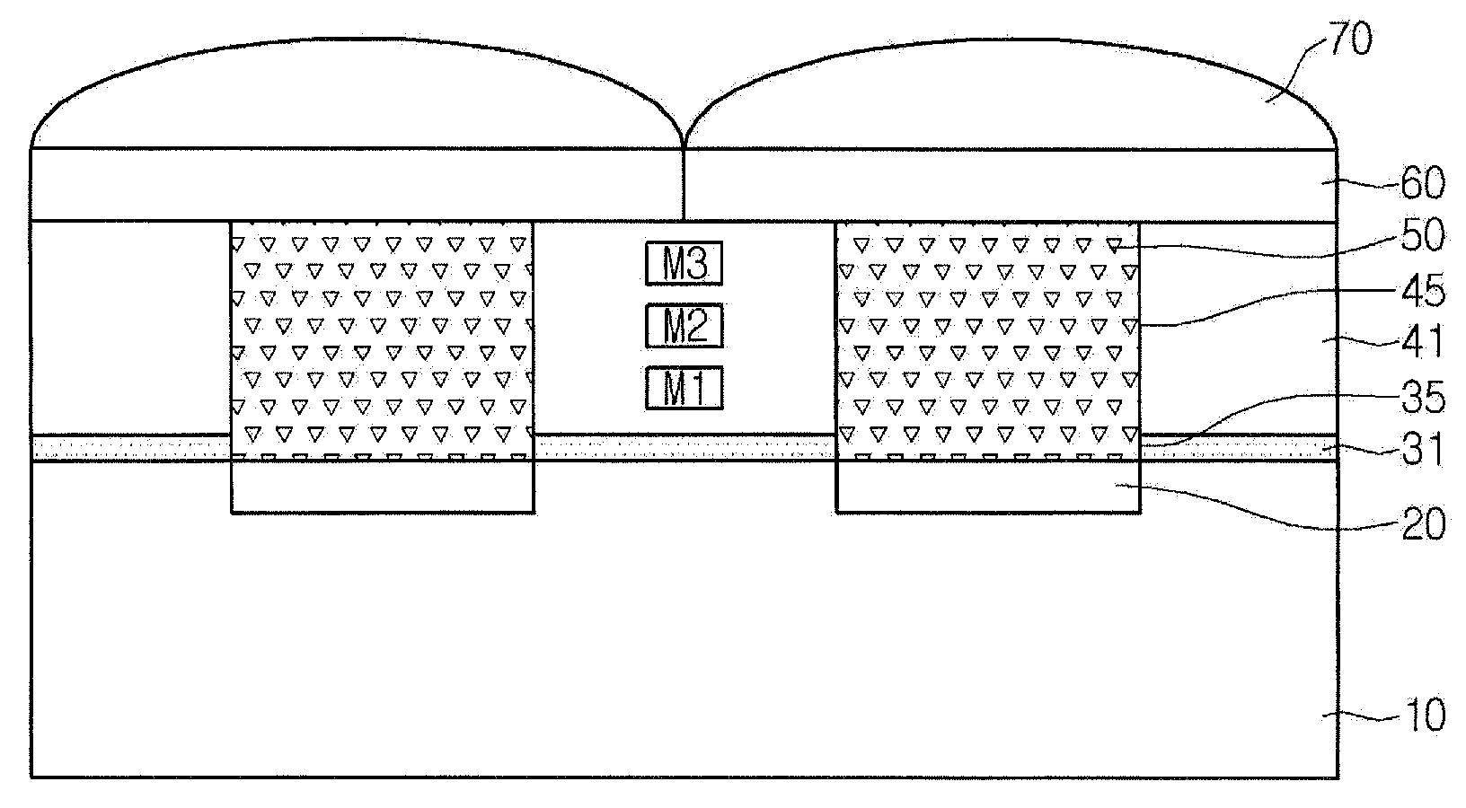
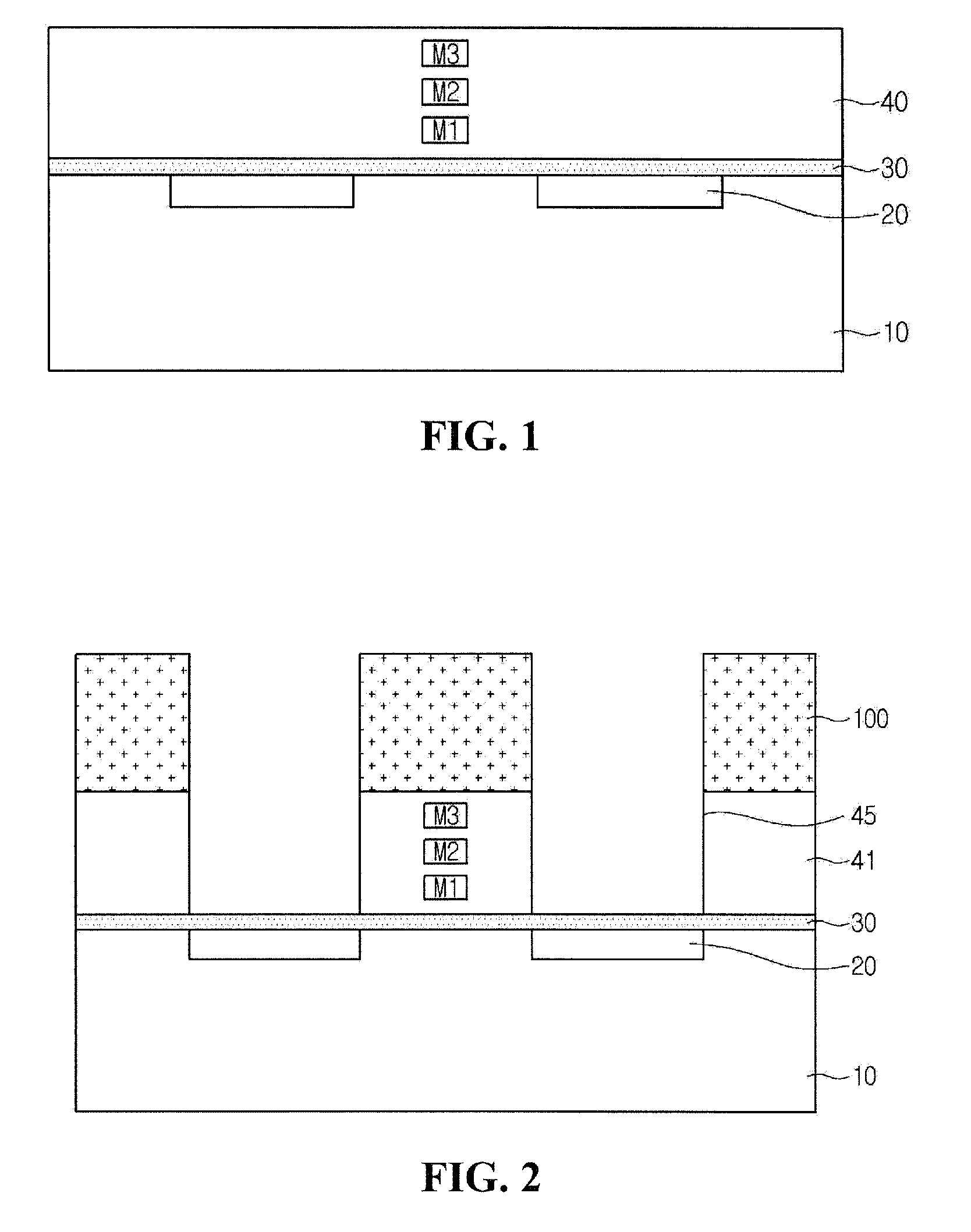
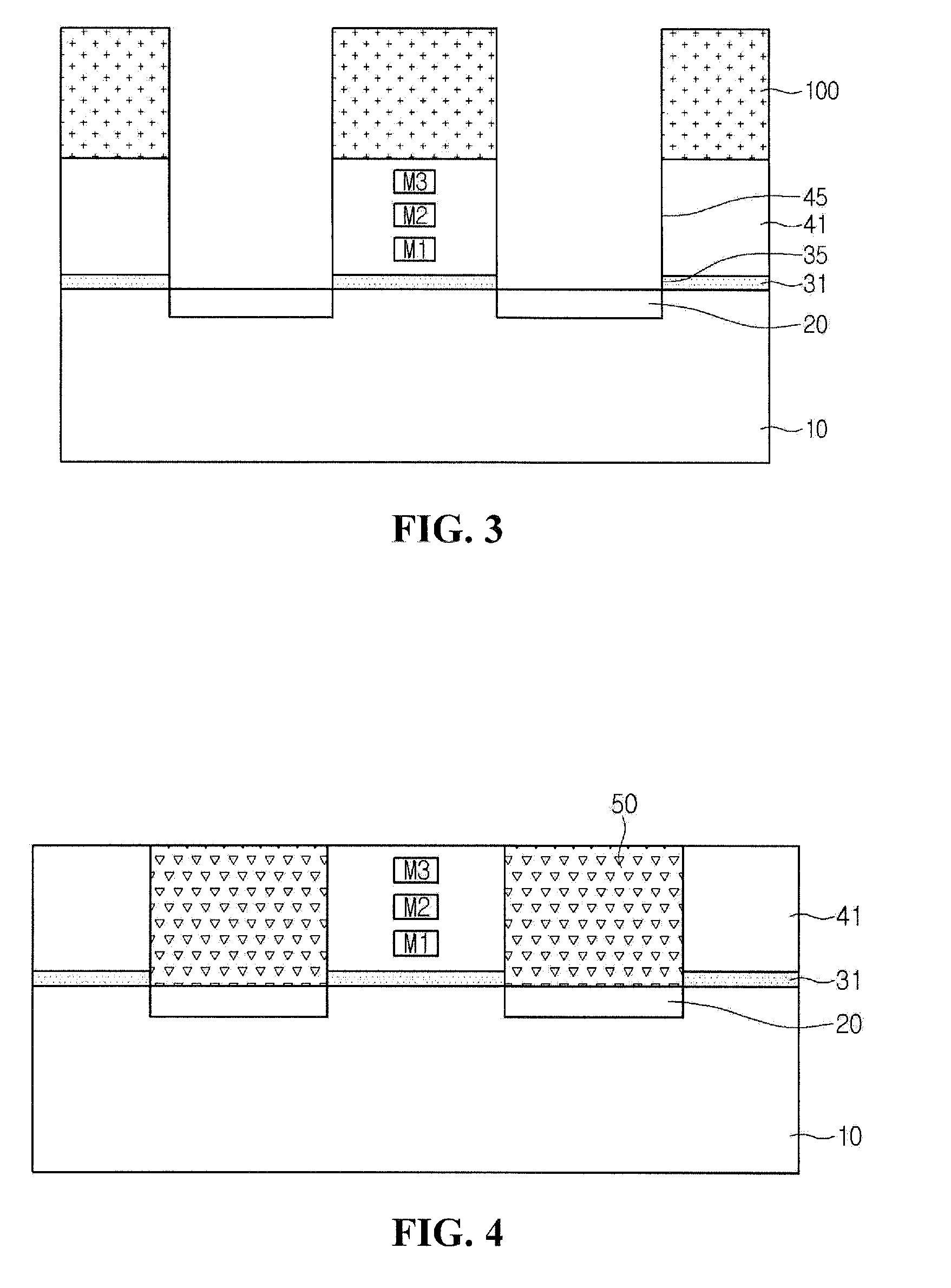
[0012]Referring to FIG. 5, an image sensor according to an embodiment can include a photodiode 20 disposed on a semiconductor substrate 10 for each unit pixel.

[0013]A protective layer pattern 31 having a ...


PUM


Abstract

An image sensor according to an embodiment includes a semiconductor substrate including a photodiode; a protective layer pattern having a lower trench that is disposed on the semiconductor substrate to expose the photodiode; an insulating layer pattern having the upper trench that is disposed on the lower trench of the protective layer pattern to expose the photodiode; and a wave guide that is disposed in the lower trench and the upper trench.

Description

CROSS-REFERENCE TO RELATED APPLICATION[0001]The present application claims the benefit under 35 U.S.C. §119 of Korean Patent Application No. 10-2007-0105939, filed Oct. 22, 2007, which is hereby incorporated by reference in its entirety.BACKGROUND[0002]An image sensor is a semiconductor device that converts an optical image into an electrical signal. Image sensors are generally classified as charge coupled device (CCD) image sensors and complementary metal oxide semiconductor (CMOS) image sensors.[0003]The CMOS image sensor utilizes a photodiode and a MOS transistor within a unit pixel to sequentially detect electrical signals of each unit pixel using a switching scheme, implementing an image.[0004]In the CMOS image sensor, as the design rule is gradually reduced, a size of a unit pixel is reduced, which can reduce photo sensitivity. In order to increase the photo sensitivity, a microlens is often formed on the color filter.[0005]However, the photo sensitivity can also be reduced by...

Claims


Application Information

Patent Timeline
IPC IPC(8): H01L31/0232H01L31/18
CPCH01L27/14629H01L27/14625H01L27/146
Inventor LEE, KANG HYUN
Owner DONGBU HITEK CO LTD
Why Eureka
Try Eureka