Light emitting device

a technology of light emitting device and light guide plate, which is applied in the direction of planar/plate-like light guide, instruments, optics, etc., can solve the problems of uneven luminance, high manufacturing cost of light guide plate, and insufficient light emitted by the light emitting element disposed in the package, so as to suppress uneven luminance.

Active Publication Date: 2009-05-07
NICHIA CORP
View PDF19 Cites 25 Cited by
  • Summary
  • Abstract
  • Description
  • Claims
  • Application Information

AI Technical Summary

Benefits of technology

[0008]Accordingly, it is an object of the present invention to provide a light emitting device that makes it possible to constitute a surface light emitting apparatus having less unevenness in luminance, without using a light guide plate made in such a configuration that does not cause unevenness in luminance or a large number of light emitting elements.
[0010]In the light emitting device of the present invention, since the opening of the recess is elongated in one direction and the angle between the side surfaces of the recess on both sides in the longitudinal direction is 90 degrees or more, light emitted by the light emitting element is spread sufficiently in the longitudinal direction of the recess so as to produce a band-shaped beam. As a result, when a plurality of light emitting elements are disposed along the longitudinal direction of the light receiving surface of the recess for constituting the surface light emitting apparatus, unevenness in luminance can be suppressed from occurring since dark portions are less likely to be generated between adjacent light emitting devices.

Problems solved by technology

However, in the case of the light emitting device of Japanese Unexamined Patent Unexamined Publication (Kokai) No. 2004-363537; and Japanese Unexamined Patent Unexamined Publication (Kokai) No. 2007-27761, it is supposed that light emitted by the light emitting element disposed in the package does not spread sufficiently along the longitudinal direction of the light receiving surface of the light guide plate.
As a result, portions between adjacent light emitting devices may remain dark, thus leading to unevenness in luminance called the firefly phenomenon, in which bright and dark portions are observed in the vicinity of the light receiving surface of the light guide plate.
While the unevenness in luminance may be eliminated by spreading the light emitted by the light emitting device uniformly over the entire light guide plate by using the light guide plate made in such a configuration that does not cause unevenness in luminance, such a light guide plate requires high manufacturing cost.
Another method of eliminating the unevenness in luminance is to dispose a large number of light emitting elements that are not packaged along the longitudinal direction of the light receiving surface of the light guide plate, although this method requires it to provide a larger number of light emitting elements for one light guide plate, thus resulting in higher cost.

Method used


Image

  • Light emitting device
  • Light emitting device
  • Light emitting device

Examples


first embodiment

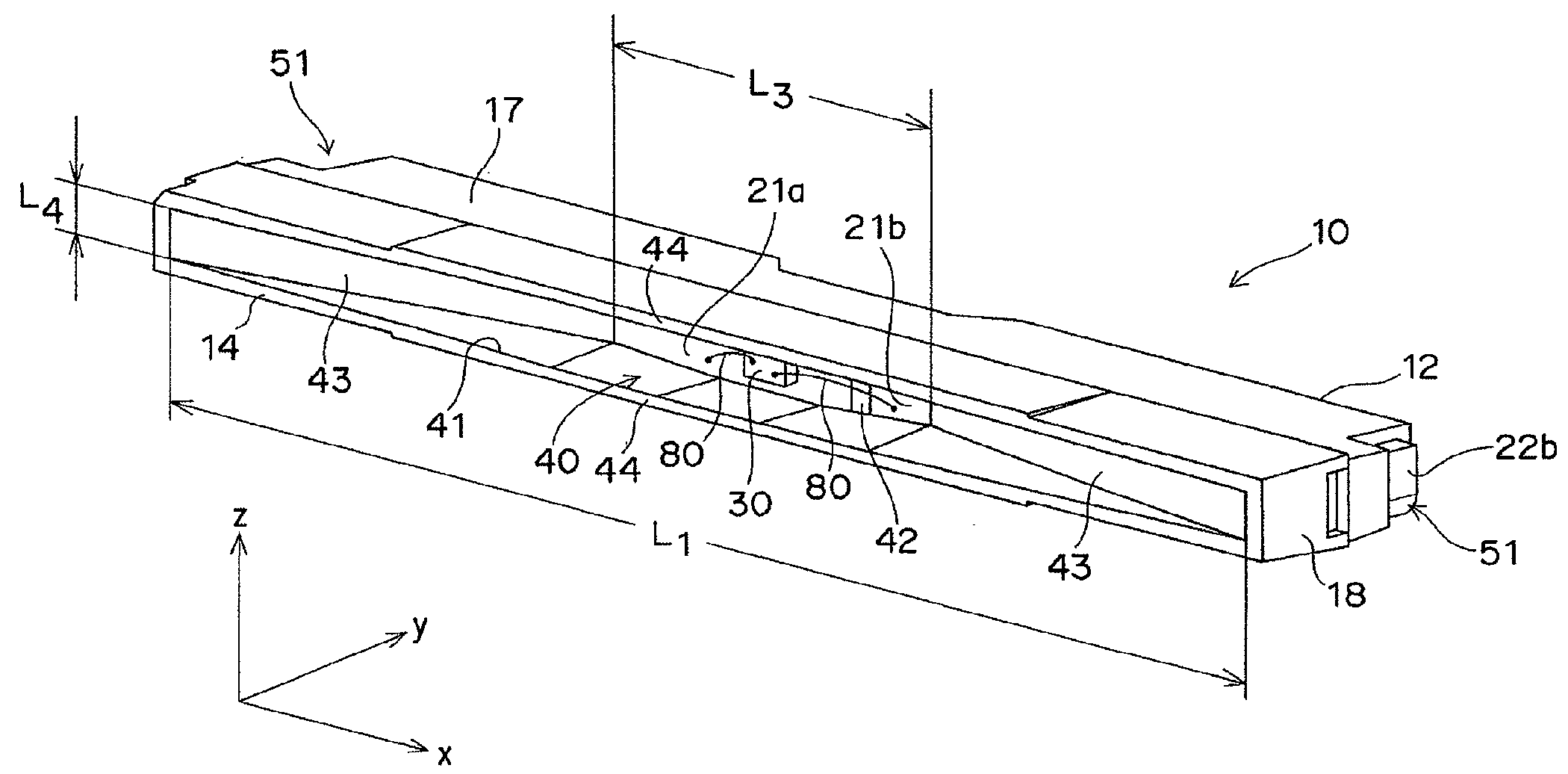
[0030]FIG. 1 and FIG. 2 show a side-view type light emitting device 10 according to this embodiment. FIG. 3 to FIG. 6 show such a state as a package 12 used in the light emitting device 10 of this embodiment is cut off from a lead frame 20. The light emitting device 10 comprises the package 12 that has a recess 40, with a light emitting element 30 mounted in the recess 40. Lead electrodes 21a, 21b are exposed as connection terminals on the bottom surface 42 of the recess 40, with part of the lead electrodes 21a, 21b penetrating through the package 12 to protrude to the outside. The light emitting element 30 and the lead electrodes 21a, 21b are connected to each other by means of electrically conductive wires 80.

[0031]The recess 40 of the package 12 opens in one surface that serves as a light emitting surface 14, and the opening 41 is elongated in one direction (x direction). Among inner side surfaces of the recess 40, the side surfaces on both sides in the longitudinal direction (x ...

second embodiment

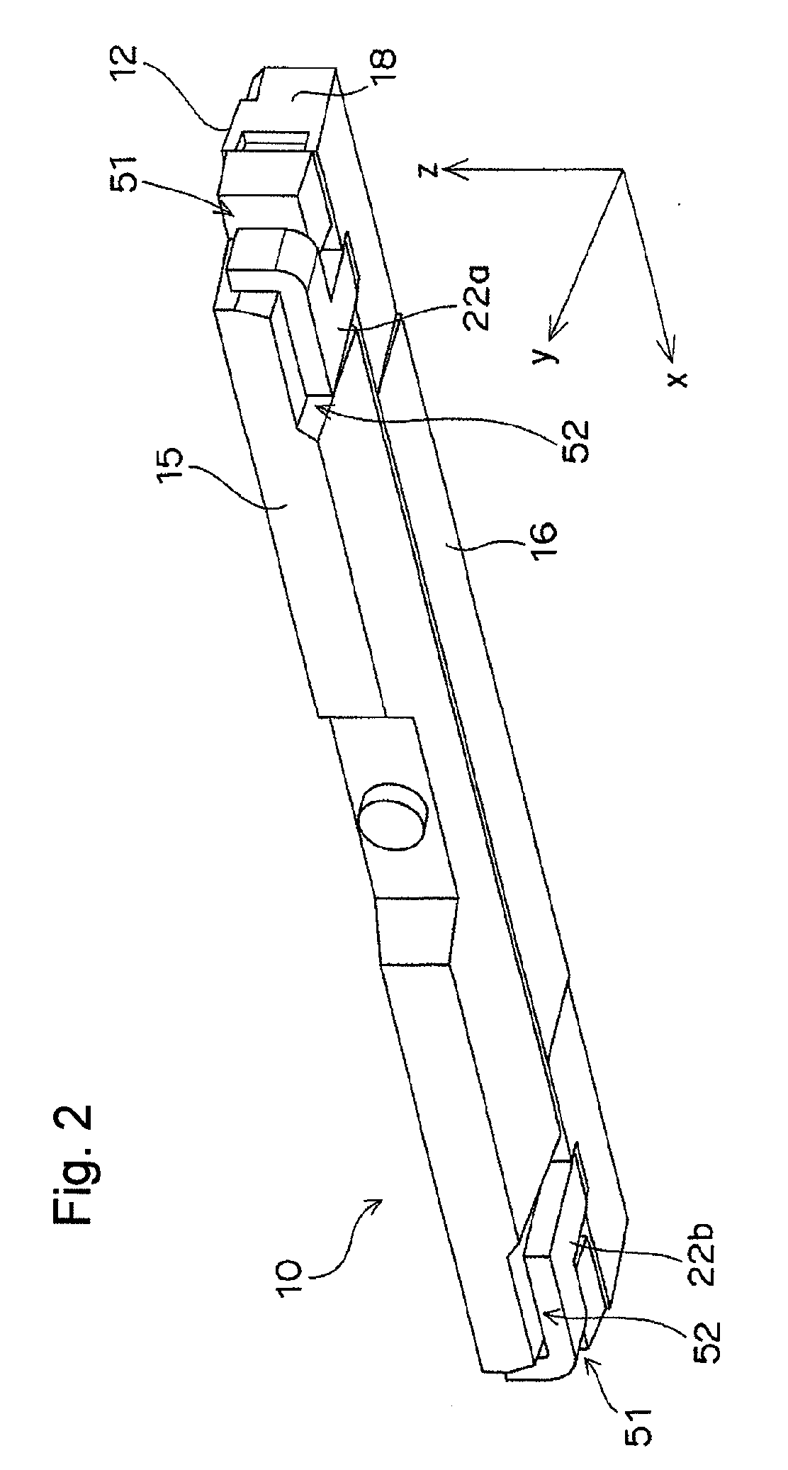
[0065]In the first embodiment described above, the step 52 (refer to FIG. 2) is formed in the mounting surface 16 of the package 12 in such a manner as the external terminals 22a, 22b can be accommodated therein when the external terminals 22a, 22b of the lead electrodes 21a, 21b are bent toward the back surface 15. The step 52 is not formed on the side of the light emitting surface 14 beyond the position where the external terminals 22a, 22b protrude from the package 12.

[0066]This embodiment is difference from the first embodiment in that the step 52 is formed also on the side of the light emitting surface 14 beyond the position where the external terminals 22a, 22b protrude from the package 12 (refer to FIG. 10). With other respects, this embodiment is the same as the first embodiment.

[0067]The step 52 is located inward from the mounting surface 16. The lead electrodes 21a, 21b protrude beyond the position of the step 52 of the mounting surface 16. That is, a boundary portion 53 b...

example 1

[0069]Luminance distribution at the center was simulated for the light emitting device 10 shown in FIG. 1. The “luminance distribution at the center” as used herein means the luminance distribution along a line that passes the center of the package 12 in the direction perpendicular to the longitudinal direction of the package 12 (z direction), and extends in the longitudinal direction of the package 12 (x direction).

[0070]Dimensions of four kinds of the light emitting device 10 (Examples 1 to 4) that were simulated are shown in Table 1.

TABLE 1Example 1Example 2Example 3Example 4Length L1 of the opening4.764.765.765.76in x direction (mm)Length L2 of the inclined1.611.642.092.12surface (mm)Length L3 of the bottom1.71.71.71.7surface (mm)Length L4 of the opening0.290.290.290.29in z direction (mm)Depth d of the recess0.50.60.50.6(mm)Angle θ between the two143.8137.2152.3147.1inclined surfaces(degrees)

[0071]For the purpose of comparison, luminance distribution at the center was simulated ...


PUM


Abstract

To provide a light emitting device that makes it possible to form a surface light emitting apparatus of less unevenness in luminance.The light emitting device 10 of the present invention comprises a light emitting element 30, connecting terminals 21a, 21b connected with the light emitting element30, a package 12 which has a recess 40 wherein the light emitting element 30 is mounted and from which a part of each connecting terminal 21a, 21b is projected outward, an opening 41 of the recess 40 being elongated in one direction, wherein both side walls of the recess 40 positioned in the longitudinal direction of the recess 40 are inclined surface 43, an angle θ between both the inclined surfaces 43 being 90 degrees or more. In the light emitting device 10 of the present invention, light emitted by the light emitting element 30 is spread sufficiently in the longitudinal direction of the opening 41 so as to produce a band-shaped beam. As a result, when a plurality of light emitting devices 10 are disposed along the longitudinal direction of the light receiving surface 72 of the light guide plate 71 for constituting the surface light emitting apparatus 70, unevenness in luminance can be suppressed from occurring as dark portions are less likely to be generated between adjacent light emitting devices 10.

Description

BACKGROUND OF THE INVENTION[0001]1. Field of the Invention[0002]The present invention relates to a light emitting device, particularly to a light emitting device suitable for backlight of liquid crystal display or the like.[0003]2. Description of the Related Art[0004]Surface light emitting apparatus, constituted from side-view type light emitting device and a light guide plate that spreads light emitted by the light emitting device into a beam having planar intensity distribution, is used as the backlight of liquid crystal display or the like. As one type of side-view type light emitting device suitable for the surface light emitting apparatus, such a low-profile light emitting device is known that has light emitting diodes disposed in a recess of a resin package having flat configuration (for example, refer to Japanese Unexamined Patent Unexamined Publication (Kokai) No. 2004-363537; and Japanese Unexamined Patent Unexamined Publication (Kokai) No. 2007-27761).[0005]A surface light...

Claims


Application Information

Patent Timeline
Patent Type & Authority Applications(United States)
IPC IPC(8): H01L33/00H01L33/62H01L33/56H01L33/60
CPCG02F1/133615H01L33/486H01L33/60G02B6/0011H01L33/62H01L2224/48091H01L2224/48247H01L2224/45147H01L2224/45144H01L2924/00014H01L2924/00H01L2224/45124H01L2224/45169H01L2924/00011H01L2924/01005
Inventor KASHIWAO, TOMOAKIKURIMOTO, TAKEO
Owner NICHIA CORP
Why Eureka
Try Eureka