

Surface-emitting display device
- Summary
- Abstract
- Description
- Claims
- Application Information
AI Technical Summary
Benefits of technology
Problems solved by technology
Method used
Image

Examples
embodiment 1
Preferred Embodiment 1
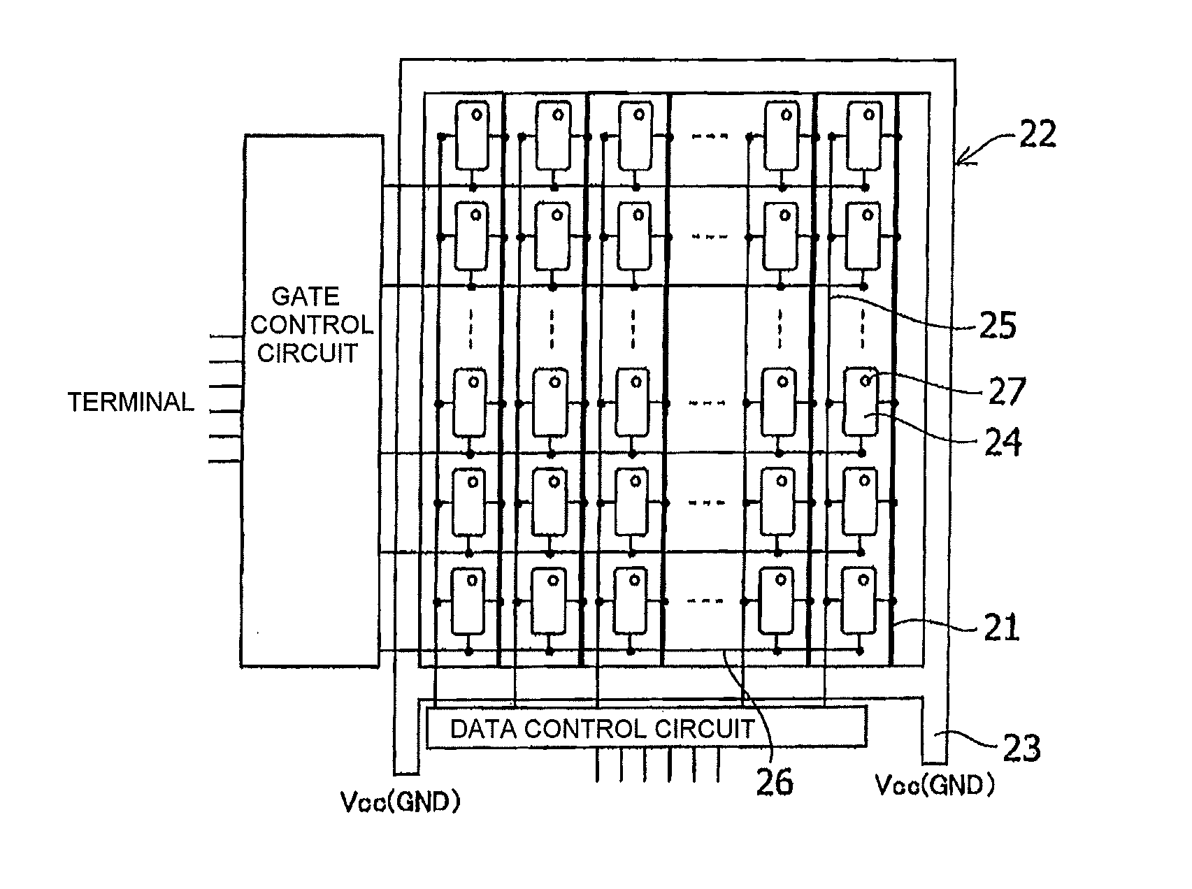
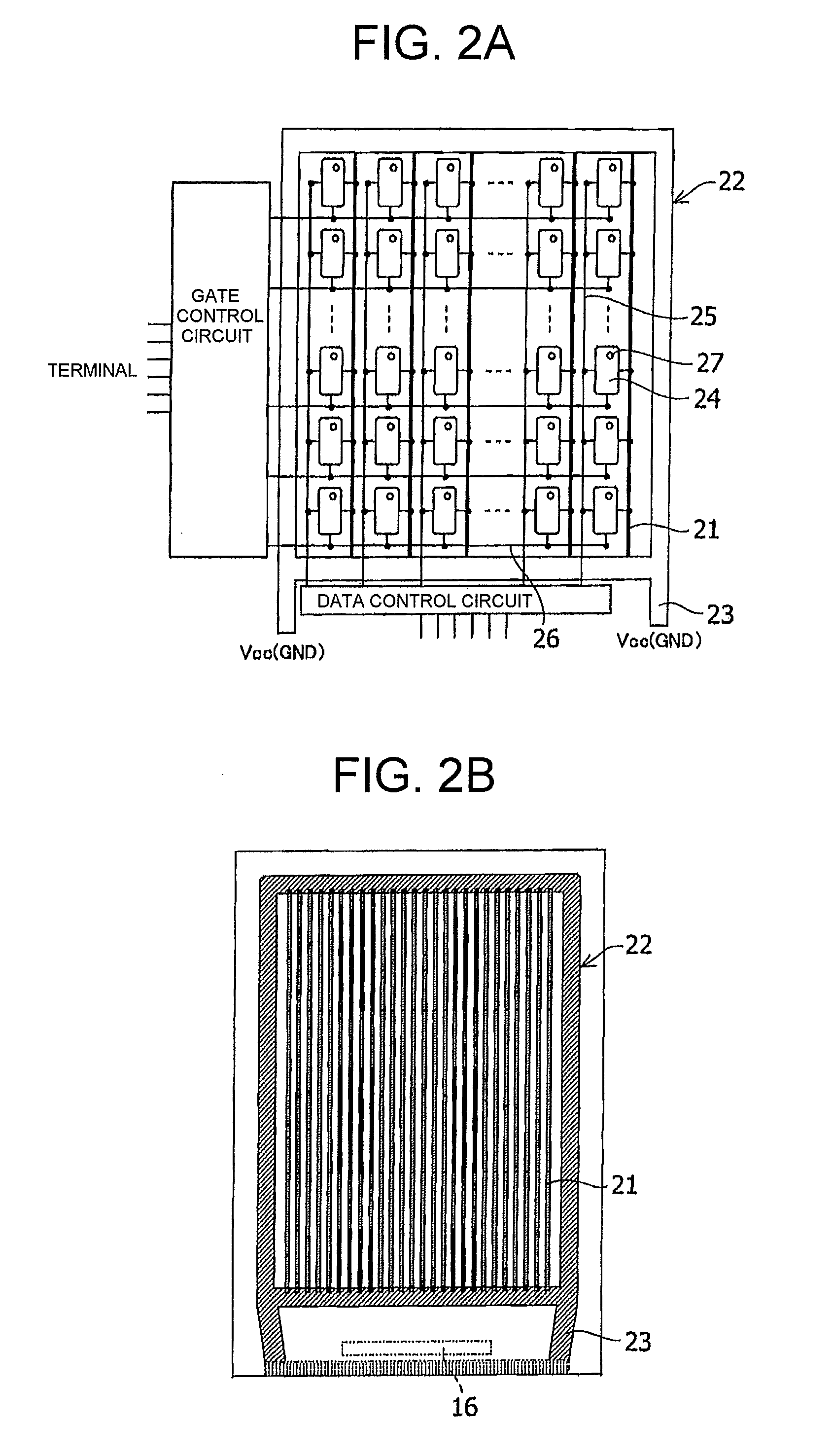
[0091]FIG. 6 is a schematic diagram of a power supply bus of this invention, and of a circuit substrate having this power supply bus. The slits 61 are narrow gaps or opening portions, and no limitations in particular are imposed on their number or length. And, the power supply bus 22 is divided into portions by these slits, and the divided portions are made thinner where connected to power supply lines closer to the power supply terminal among the plurality of power supply lines 21, and are made thicker where connected to more distant power supply lines. The symbol 62 indicates multilayer wiring portions in which the power supply bus has a layered structure. Portions of the power supply bus not intersecting with data signal lines or gate signal lines can be provided with a structure in which the same metal is layered. It is desirable that this structure have lateral symmetry.
[0092]Ideally, so-called constant-resistance wiring would be used, in which a power sup...
embodiment 2
Preferred Embodiment 2
[0098]Next, FIG. 12 through FIG. 16 are used to explain a circuit substrate in which, in addition to the power supply bus having slits of FIG. 6 through FIG. 9, connection lines are also added to connect together power supply lines.
[0099]FIG. 12 is a schematic diagram of a circuit substrate including the power supply bus of FIG. 6 through FIG. 9 and connection lines 63 which connect together power supply lines 21. Here, arbitrary values can be used for the number and lengths of the slits provided in the power supply bus 22 of FIG. 12, and no limitations in particular are imposed. It is important that slits 61 be formed such that the power supply bus is divided into portions, and that the divided portions are thinner where connected to power supply lines near the power supply terminal, and are thicker where connected to more distance power supply lines. And, the connection lines 63 connect together power supply lines 21 which are adjacent in the direction perpen...
embodiment 3
Preferred Embodiment 3
[0116]FIG. 17 through FIG. 19 show an example of a TFT circuit substrate in which a bypass line path to reduce wiring resistance of power supply lines 210 has been added to the configuration of FIG. 14 through FIG. 16. This example focuses on the fact that the source wiring pattern 56a of FIG. 15 is at the same potential as the cathode. As shown in FIG. 18, this bypass line path is formed connecting the source wiring pattern 56 to the connection line 59 via the contact hole 60a. Hence compared with the configuration of FIG. 14 through FIG. 16, in addition to effective utilization of space, wiring resistance of the power supply line 210 can be reduced. This bypass line path is disclosed in an international patent application (PCT / JP2008 / 061967) submitted by the applicant of this application on Jul. 2 2008, and the contents thereof are incorporated into this specification by reference.
[0117]As the manufacturing process for FIG. 17 through FIG. 19, the manufacturi...
PUM
 Abstract
Description
Claims
Application Information