OLED display and production method thereof

A manufacturing method and display technology, applied in semiconductor/solid-state device manufacturing, electric solid-state devices, semiconductor devices, etc., can solve problems such as cross-color, low brightness, and sub-pixel light-emitting effects, so as to reduce uneven brightness and avoid cross-color Phenomenon, the effect of reducing the sheet resistance

Inactive Publication Date: 2018-02-23
SHENZHEN CHINA STAR OPTOELECTRONICS SEMICON DISPLAY TECH CO LTD
View PDF15 Cites 34 Cited by
  • Summary
  • Abstract
  • Description
  • Claims
  • Application Information

AI Technical Summary

Problems solved by technology

However, the transparent cathode and semi-transparent cathode with the above resistance values ​​are only suitable for use in small-size displays. When used in large-size displays, the voltage drop (IR drop) will occur due to the high square resistance of the cathode, which will cause the display to appear. The phenomenon of uneven brightness, and the farther away from the cathode voltage input terminal, the lower the brightness
In addition, whether it is an OLED device with a white light emitting layer (White OLED structure) or an OLED device with a red, green and blue light emitting layer (RGB side-by side), there are some common layers (common layer), such as the hole injection layer ( HIL), Hole Transport Layer (HTL), Electron Transport Layer (ETL), Electron Injection Layer (EIL), and Carrier Generation Layer (CGL), etc. These common layers are all made using Openmask, Covering all sub-pixel regions and the space between sub-pixels, because some common layer materials have better carrier transport properties, carriers will conduct laterally in these common layers, causing the common layer to generate lateral leakage. When a When a sub-pixel is lit, its adjacent sub-pixels are easily affected by the current in the sub-pixel, resulting in uncontrollable brightness, resulting in cross-color phenomenon
[0006] figure 1 It is a schematic diagram of the lateral leakage of the common layer of the existing OLED substrate, such as figure 1 As shown, the OLED light-emitting layer 100 in the OLED substrate is a white light-emitting layer, and the OLED light-emitting layer 100 (including the hole injection layer, the hole transport layer, the light-emitting layer, the electron transport layer and the electron transport layer) of all sub-pixels of the OLED substrate Injection layers) communicate with each other and appear as a common layer. When lateral leakage occurs inside the OLED light-emitting layer 100, carriers move laterally in the OLED light-emitting layer 100, from one sub-pixel to an adjacent sub-pixel. The light emission of adjacent sub-pixels is affected, resulting in uncontrollable brightness of the adjacent sub-pixels. When the OLED substrate cooperates with color filters to realize screen display, cross-color phenomenon is prone to occur.

Method used


Image

  • OLED display and production method thereof
  • OLED display and production method thereof
  • OLED display and production method thereof

Examples


Embodiment Construction

[0067] In order to further illustrate the technical means adopted by the present invention and its effects, the following describes in detail in conjunction with preferred embodiments of the present invention and accompanying drawings.

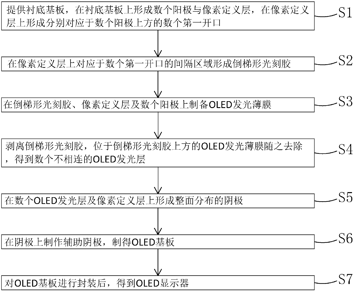
[0068] see figure 2 , the invention provides a method for manufacturing an OLED display, comprising the steps of:

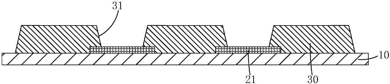
[0069] Step 1, such as image 3 As shown, a base substrate 10 is provided, and several anodes 21 arranged in an array are formed on the base substrate 10, and a pixel definition layer 30 is formed on the base substrate 10 and the plurality of anodes 21. A plurality of first openings 31 corresponding to the plurality of anodes 21 are formed on the pixel definition layer 30 .

[0070] Specifically, the base substrate 10 is a TFT substrate.

[0071] Specifically, the step 1 further includes: forming a flat layer (not shown) between the base substrate 10 and several anodes 21 .

[0072] Specifically, the areas of the plurality o...


PUM


Abstract

The invention provides an OLED display and a production method thereof. According to the production method of the OLED display, by means of photoresists in a shape of an inverted trapezium arranged inspacer areas of multiple sub-pixels, the effect that multiple OLED illuminating layers are not connected with one another is achieved, and the situation of lateral electric leakage of common layers does not happen to the obtained OLED display, so that the cross color phenomenon caused by migration of carriers between the adjacent sub-pixels is avoided, and it is guaranteed that the OLED display has a good display effect; moreover, by producing auxiliary negative electrodes which are connected with negative electrodes over or under the negative electrodes, the square resistance of the negativeelectrodes can be reduced, and then the problem of uneven brightness caused by voltage drops is solved. The OLED display is obtained by adopting the method, and the cross color phenomenon does not happen, so that the OLED display has a good display effect; the auxiliary electrodes which are connected with the negative electrodes are arranged over or under the negative electrodes, so that the square resistance of the negative electrodes is reduced, and then the problem of uneven brightness caused by the voltage drops is solved.

Description

technical field [0001] The invention relates to the field of display technology, in particular to an OLED display and a manufacturing method thereof. Background technique [0002] Organic Light Emitting Display (OLED) has self-illumination, low driving voltage, high luminous efficiency, short response time, high definition and contrast, nearly 180° viewing angle, wide operating temperature range, and can realize flexible display and With many advantages such as large-area full-color display, it is recognized by the industry as a display device with the most potential for development. [0003] According to the driving method, OLED can be divided into two categories: passive matrix OLED (Passive Matrix OLED, PMOLED) and active matrix OLED (Active Matrix OLED, AMOLED), namely direct addressing and thin film transistor matrix addressing. Among them, AMOLED has pixels arranged in an array, belongs to the active display type, has high luminous efficiency, and is usually used as a...

Claims


Application Information

Patent Timeline
Patent Type & Authority Applications(China)
IPC IPC(8): H01L27/32H01L21/77
CPCH01L21/77H10K59/00H10K59/122H10K71/221H10K50/824H10K71/00
Inventor 方俊雄吴元均
Owner SHENZHEN CHINA STAR OPTOELECTRONICS SEMICON DISPLAY TECH CO LTD
Why Eureka
Try Eureka