Method of manufacturing silicon nanotubes using doughnut-shaped catalytic metal layer

a technology of metal layer and silicon nanotube, which is applied in the direction of nanoinformatics, silicon compounds, crystal growth process, etc., can solve the problems of difficult control as desired, and achieve the effect of efficient manufacturing and efficient manufacturing

Inactive Publication Date: 2009-05-14
ELECTRONICS & TELECOMM RES INST
View PDF6 Cites 5 Cited by
  • Summary
  • Abstract
  • Description
  • Claims
  • Application Information

AI Technical Summary

Benefits of technology

[0015]According to the present invention, the silicon nanotube can be efficiently manufactured by growing the silicon nanotube using the catalyst metal doughnuts. According to the present invention, silicon nanotubes can be efficiently manufactured by growing the silicon nanotubes using catalyst metal doughnuts instead of simply using a catalytic metal layer used in the manufacture of carbon nanotubes.

Problems solved by technology

Carbon nanotubes have both semiconductor and metal characteristics and such characteristics are hard to control as desired when the carbon nanotubes are manufactured.

Method used


Image

  • Method of manufacturing silicon nanotubes using doughnut-shaped catalytic metal layer
  • Method of manufacturing silicon nanotubes using doughnut-shaped catalytic metal layer
  • Method of manufacturing silicon nanotubes using doughnut-shaped catalytic metal layer

Examples


Embodiment Construction

[0022]Hereinafter, the present invention will be described more fully with reference to the accompanying drawings, in which exemplary embodiments of the invention are shown. The invention may, however, be embodied in many different forms and should not be construed as being limited to the embodiments set forth herein; rather, these embodiments are provided so that this disclosure will be thorough and complete, and will fully convey the concept of the invention to those skilled in the art. In the drawings, like reference numerals denote like elements, and the sizes and thicknesses of layers and regions are exaggerated for clarity.

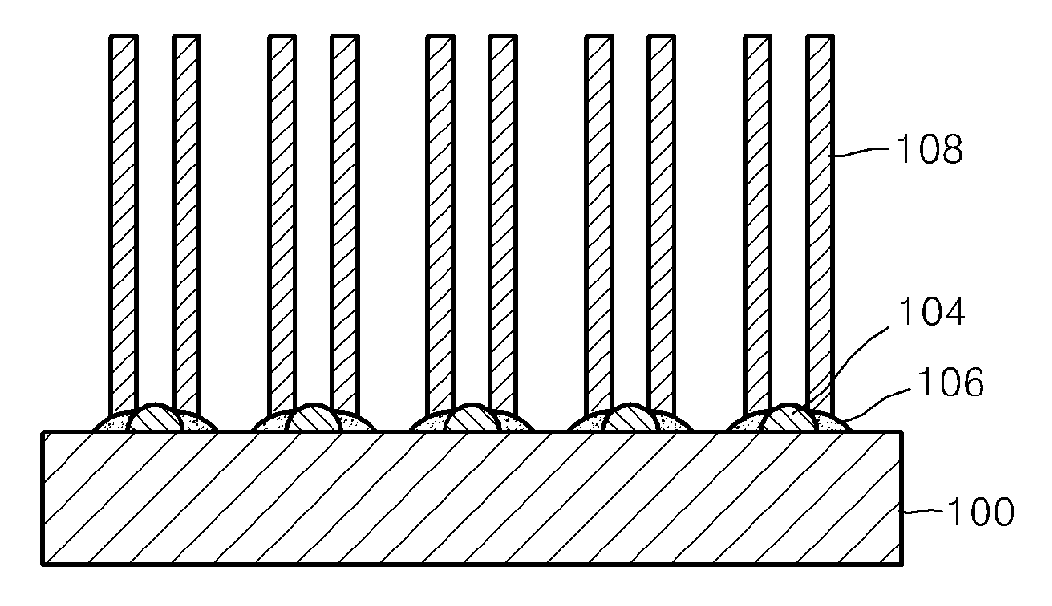
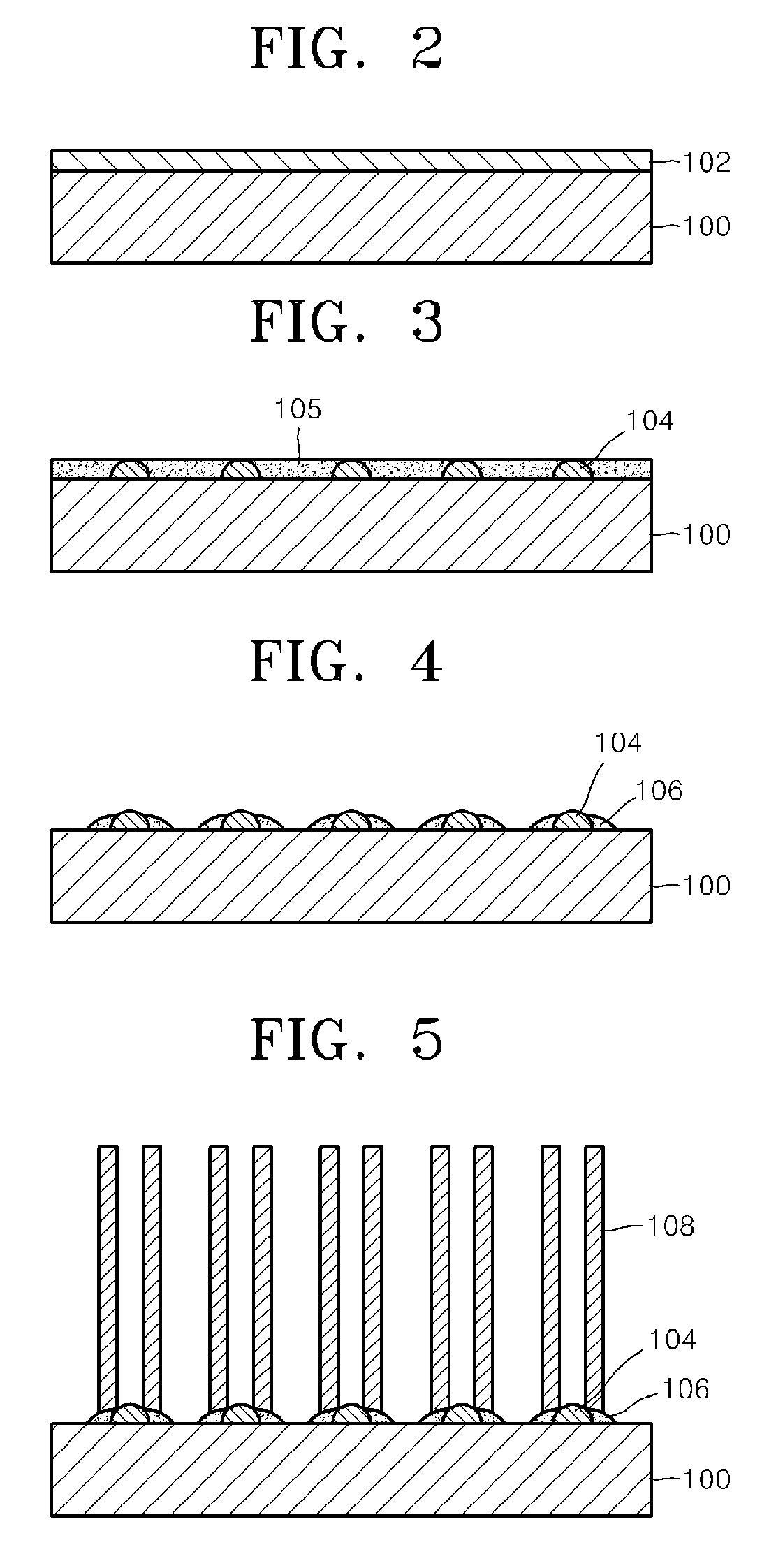
[0023]As described in the ‘Description of the Related Art’ of the present invention, when a method of manufacturing carbon nanotubes is used to grow silicon nanotubes, the silicon nanotubes grow into nanowires, instead of nanotubes. However, according to an embodiment of the present invention, a doughnut-shaped catalytic metal layer is used to grow the silic...


PUM

PropertyMeasurementUnit
thicknessaaaaaaaaaa
thicknessaaaaaaaaaa
thicknessaaaaaaaaaa

Abstract

Provided is a method of manufacturing silicon nanotubes including forming non-catalytic metal islands on a substrate; forming catalyst metal doughnuts to surround the non-catalytic metal islands; and growing silicon nanotubes on the catalyst metal doughnuts. The silicon nanotubes are efficiently grown using the catalyst metal doughnuts.

Description

TECHNICAL FIELD[0001]The present invention relates to a method of manufacturing nanotubes and more particularly, to a method of manufacturing silicon nanotubes.BACKGROUND ART[0002]Carbon nanotubes are widely used in new high-speed and highly-integrated electrical components or sensors. Carbon nanotubes can be manufactured by thermal chemical vapor deposition in suitable growth conditions using a catalytic metal layer. Carbon nanotubes have both semiconductor and metal characteristics and such characteristics are hard to control as desired when the carbon nanotubes are manufactured.[0003]As a result of this, silicon nanotubes have been developed. In general, silicon has semiconductor characteristics and thus, silicon nanotubes can be used in electric components and sensors. In addition, similar to carbon nanotubes, characteristics of silicon nanotubes are determined by the structure of the outer walls thereof. Silicon nanotubes have characteristics that are not known up to now and ma...

Claims


Application Information

Patent Timeline
Patent Type & Authority Applications(United States)
IPC IPC(8): C23C16/24
CPCB82Y10/00H01L29/16C01B33/02C01B33/027C30B25/00C30B29/06C30B29/602H01L21/02532H01L21/02606H01L21/0262H01L21/02639H01L21/02642H01L21/02645H01L21/02653H01L29/0665H01L29/0673H01L29/0676B82Y30/00B82B3/00B82Y40/00
Inventor PARK, RAE-MANSANG-HYOOB, KIMMAENG, SUNGLYULPARK, JONGHYURK
Owner ELECTRONICS & TELECOMM RES INST
Why Eureka
Try Eureka