Adjustable Mask Blank Structure for an Euv Phase-Shift Mask

a phase shift mask and mask blank technology, applied in the field of optical components, can solve the problems of difficult control of etching to within 1 , difficult control of step thickness

Inactive Publication Date: 2009-05-21
COMMISSARIAT A LENERGIE ATOMIQUE ET AUX ENERGIES ALTERNATIVES
View PDF4 Cites 47 Cited by
  • Summary
  • Abstract
  • Description
  • Claims
  • Application Information

AI Technical Summary

Problems solved by technology

Technologically, control over etching to within ±1 Å is very difficult.
Therefore the problem that arises is to control step thicknesses for manufacturing of optical components, and particularly phase shift EUV masks, to within an Angstrom.

Method used


Image

  • Adjustable Mask Blank Structure for an Euv Phase-Shift Mask
  • Adjustable Mask Blank Structure for an Euv Phase-Shift Mask
  • Adjustable Mask Blank Structure for an Euv Phase-Shift Mask

Examples


example 2

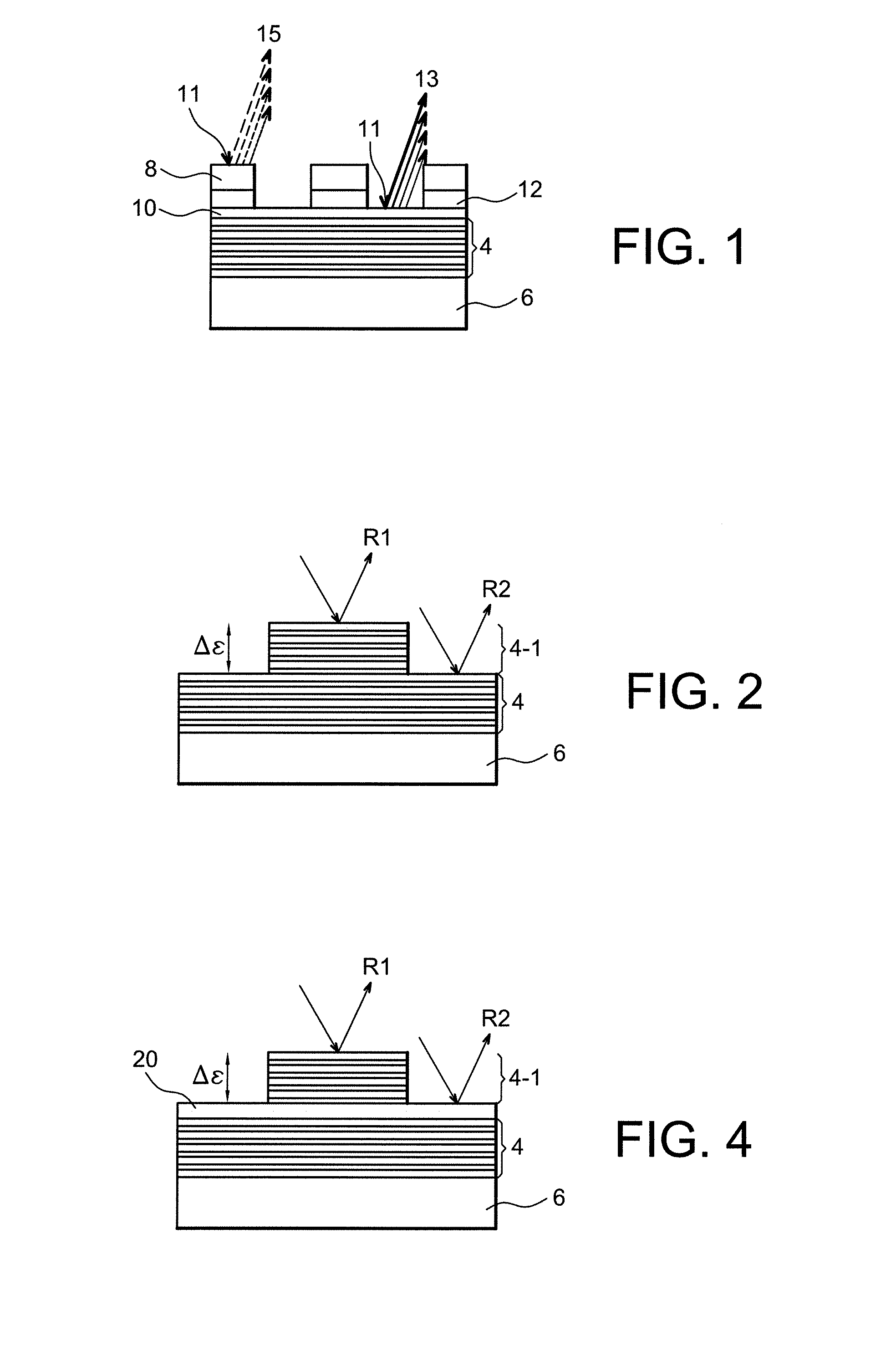
[0108]The adjustment layer 30 comprises a bilayer pair Mo—Si, each bilayer comprising a 2 nm layer of Si and a 1.5 nm layer of Mo. Other parameters are identical to the parameters in example 1. The advantage is that in this case, there are two interdiffusion zones Mo—Si, therefore a double contraction effect in comparison with FIG. 1, all other things being equal.

example 3

[0109]The adjustment layer 30 is a mix of Mo and Si obtained by co-sputtering or co-evaporation of molybdenum and silicon; the deposition rates are adjusted so as to deposit twice much as Si as Mo: the result is thus a composite material comprising either a single phase of amorphous MoSi2, or a phase of amorphous Si with Mo aggregates, or both at the same time. An appropriate annealing will cause contraction of the adjustment layer by homogenising this layer of amorphous MoSi2.

example 4

[0110]This example is exactly the same as examples 1 or 2, except that Mo is replaced by Ru in the stack 30. The advantage is that diffusion of Si in Ru takes place at a lower temperature than in Mo (see table II). The adjustment by annealing is made under less restrictive conditions for the multi-layer mirror function 32, 34.


PUM

PropertyMeasurementUnit
temperatureaaaaaaaaaa

Abstract

The invention concerns a process for forming an optical component comprising:
    • a—formation of a multi-layer stack (32, 34) with an adjustment layer (30) made of a metal-semiconductor mix formed in or on the stack,
    • b—etching a part of the multi-layer stack, including at least a part of the adjustment layer,
    • c—an annealing step to contract the adjustment layer within less than 1 nm.

Description

TECHNICAL DOMAIN AND PRIOR ART[0001]The invention relates to the domain of optical components, and particularly but not uniquely, mask blanks and lithography masks for microelectronic application, for example EUV masks operating in reflection or phase shift masks.[0002]The spectral application domain is preferably the Extreme Ultra-Violet (EUV: λ=10-30 nm).[0003]One example of an application domain is EUV lithography in microelectronics.[0004]The invention also relates to EUV optical functions requiring a fine adjustment of the thickness of the optical structure within a variation range between 1 Å and a few nanometers.[0005]In general, in the domain of lithography masks, the size of patterns to be printed on the silicon wafer is reduced firstly by reducing the insulation wavelengths, and secondly by optimisation of the optical structure of masks.[0006]In principle, the objective is to project increasingly small patterns on the resin covering the silicon wafer, with contours as well...

Claims


Application Information

Patent Timeline
Patent Type & Authority Applications(United States)
IPC IPC(8): G21K5/00G03F1/00G03C5/00
CPCB82Y10/00B82Y40/00G03F1/24G03F7/70566G03F7/70283G03F7/70308G03F1/34
Inventor QUESNEL, ETIENNE
Owner COMMISSARIAT A LENERGIE ATOMIQUE ET AUX ENERGIES ALTERNATIVES
Why Eureka
Try Eureka