Semiconductor device and method for production thereof

a technology of semiconductor devices and integrated circuits, applied in semiconductor devices, semiconductor/solid-state device details, electrical apparatus, etc., can solve the problems of increasing the number of steps, increasing the gate resistance, and deteriorating the performance of elements, and achieves simplified process, simplified process, and excellent element characteristics

Inactive Publication Date: 2009-05-21
ELPIDA MEMORY INC
View PDF3 Cites 2 Cited by
  • Summary
  • Abstract
  • Description
  • Claims
  • Application Information

AI Technical Summary

Benefits of technology

[0021]It is an object of the present invention to provide a semiconductor device capable of production with a simple process while having a polymetal gate structure and having a metal silicide layer for contact on a source-drain region, and a method for production thereof.
[0082]According to the present invention, a semiconductor device capable of production with a simple process while having a polymetal gate structure and having a metal silicide layer for contact on a source-drain region, and a method for production thereof can be provided. In particular, according to the present invention, the gate contact is not connected directly to a metal layer that forms the gate electrode upper layer part, but connected to a polysilicon layer that forms the gate electrode lower layer part via a metal silicide formed on the surface of the substrate. Thus, even if holes for a gate contact and a source-drain contact are formed at the same time, a gate electrode structure can satisfactorily be formed, and resultantly, a semiconductor device excellent in element characteristics can be produced with a simplified process.

Problems solved by technology

However, when the gate length is reduced, the gate resistance increases, and in a conventional polycide gate, the gate resistance increases, and the element performance is deteriorated.
If a step of forming a hole for contact with a source-drain region and a step of forming a hole for contact with a gate electrode are separately carried out to form contacts, respectively, as described above, there is a problem of increasing the number of steps.
However, if contacts are formed after forming both the holes formed for simplifying a production process, the following problem arises.

Method used


Image

  • Semiconductor device and method for production thereof
  • Semiconductor device and method for production thereof
  • Semiconductor device and method for production thereof

Examples


first embodiment

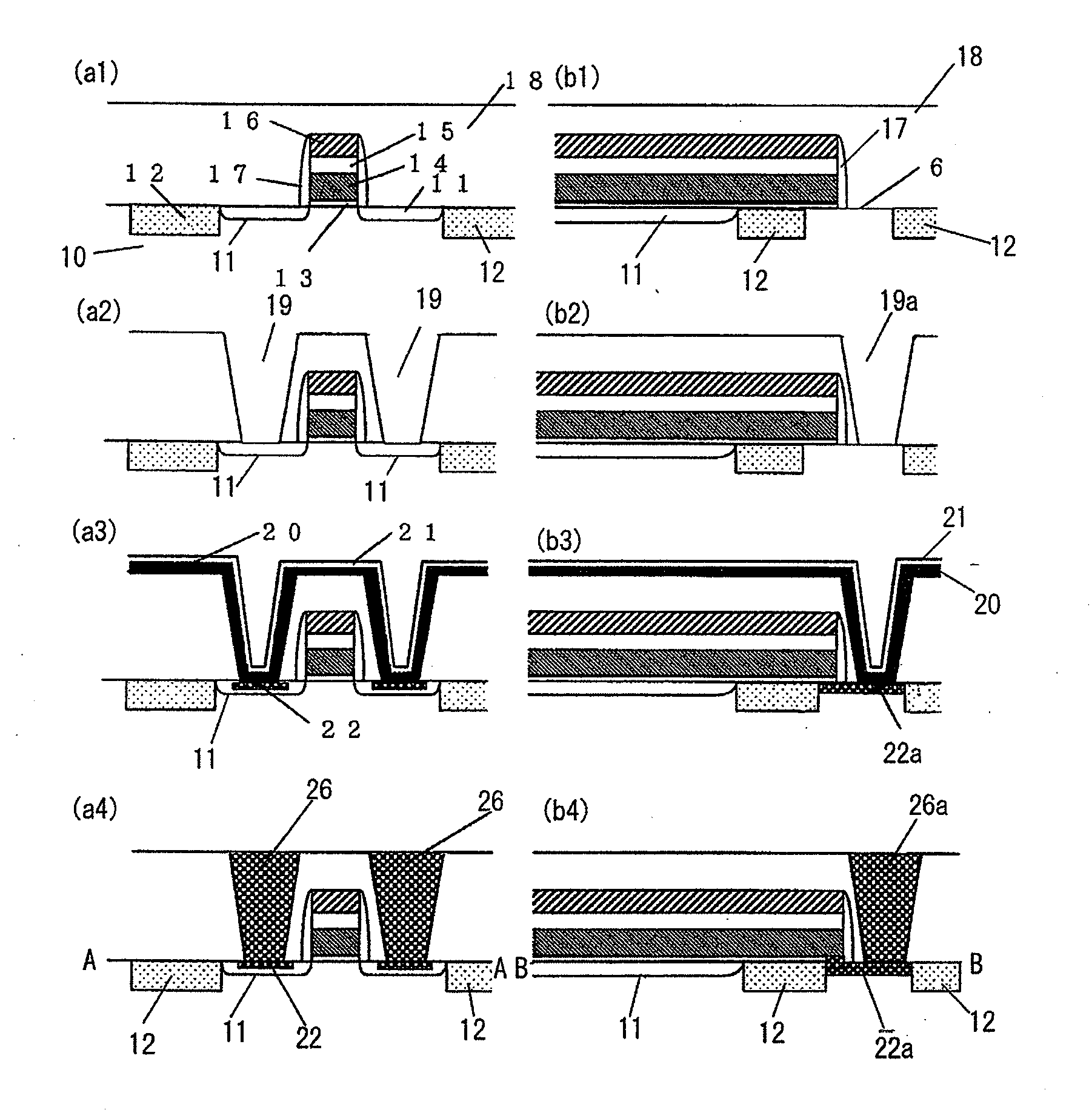
[0095]the present invention will be further described using FIGS. 3 and 4(a1) to 4(a4) and 4(b1) to 4(b4).

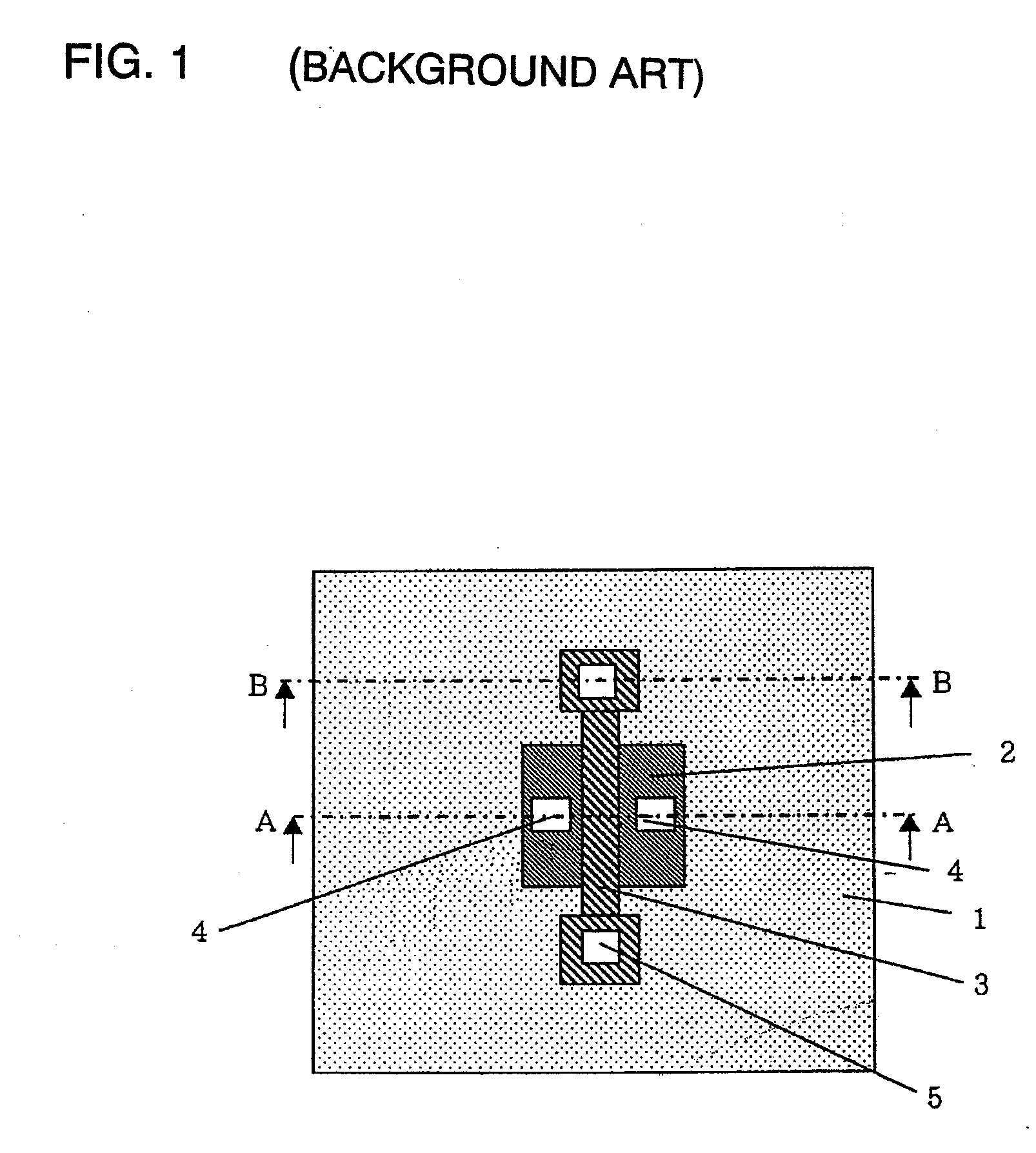
[0096]FIG. 3 is a schematic plan view of a unit element of an FET constituting the semiconductor device of this embodiment. An active region for forming an FET element, element isolating region 1 and contact forming region 6 for forming a gate contact are formed on the silicon substrate. The gate electrode 3 extends to the top of the element isolating region from the top of the active region, and further, an end portion of gate electrode 3 reaches and partly overlaps with the top of contact forming region 6. Gate contact plug 26a is provided so as to contact the top surface of the substrate in the contact forming region. Diffusion layer region 2 as a source-drain region is formed on the active region, and source-drain contact 4 is provided on the region.

[0097]FIGS. 4(a1) to 4(a4) are process sectional views taken along line A-A of FIG. 3, and FIGS. 4(b1) to 4(b4) are process sec...

second embodiment

[0130]The second embodiment will be described in detail using FIG. 6.

[0131]FIGS. 6(a) and 6(b) correspond to FIGS. 4(a2) and 4(b2) of the first embodiment, respectively. In this embodiment, contact diameter d2 of hole 19a is smaller than contact diameter d1 of hole 19.

[0132]When a hole is formed in an interlayer insulating film using the anisotropic dry etching method, damage by dry etching is left on the surface of the substrate at the bottom of the hole. According to a chemical dry etching (CDE) method, this damage can be removed.

[0133]In this embodiment, for removing the damage layer at the bottom of hole 19 by dry etching, the silicon surface exposed at the bottom of the hole is removed by 10 nm using a CDE method under the conditions described below, and the damage layer at the bottom of hole 19a is left without being removed.

[0134]For the CDE method, a mixed gas of O2 / CF4 may be used.

[0135]Since opening diameter d2 of hole 19a is smaller than opening diameter d1 of hole 19 and...

third embodiment

[0138]The third embodiment will be described.

[0139]In this embodiment, the gate insulating film formed on contact forming region 6 is made to have a thickness smaller than that of the gate insulating film formed on the active region in the structure shown in FIG. 4(b1). The thickness of the gate insulating film formed on contact forming region 6 may be set to, for example, 5 nm whereas the thickness of the gate insulating film formed on the active region is 10 nm.

[0140]A structure in which the thickness of the gate insulating film varies depending on the region can be formed by a publicly known method known as a multi-oxide process. For example, by carrying out a process comprising a first oxide film forming step of forming an oxide film on a first region and a second region, a step of masking the second region and removing the oxide film on the first region, and a second oxide film forming step of forming an oxide films on the first region and the second region after removing the m...


PUM


Abstract

A semiconductor device having a silicon substrate, an element isolating film, an active region, a gate electrode provided via a gate insulating film, a diffusion layer provided on the active region on opposite sides of the gate electrode, an interlayer insulating film, and a plug filled in a hole formed on the interlayer insulating film, wherein the semiconductor device further has a contact forming region surrounded by the element isolating film, and a conductive layer formed on the contact forming region, the gate electrode extends so as to overlap with a portion of the contact forming region and is connected to the conductive layer at the overlapping portion, and the plug contacts the conductive layer at another portion of the contact forming region and is electrically connected to the gate electrode via the conductive layer.

Description

[0001]This is a divisional of application Ser. No. 11 / 585,165 filed Oct. 24, 2006, which claims priority from Japanese Patent Application Nos. 2005-311286 and 2006-221003 filed Oct. 26, 2005 and Aug. 14, 2006. The entire disclosures of the prior applications, are considered part of the disclosure of the accompanying divisional application and are hereby incorporated by reference.BACKGROUND OF THE INVENTION[0002]1. Field of the Invention[0003]The present invention relates to a semiconductor device and a method for production thereof, and relates particularly to a semiconductor integrated circuit device having a polymetal gate structure and a method for production thereof.[0004]2. Description of the Related Art[0005]In recent years, semiconductor integrated circuit devices, for example MPUs (microprocessors: micro processing units) for use in personal computers have had their computing speed improved by reducing the gate electrode width and increasing the drive frequency. The gate ele...

Claims


Application Information

Patent Timeline
Patent Type & Authority Applications(United States)
IPC IPC(8): H01L21/283
CPCH01L21/76895H01L23/485H01L29/4238H01L29/78H01L2924/0002H01L2924/00
Inventor HASUNUMA, EIJI
Owner ELPIDA MEMORY INC
Why Eureka
Try Eureka