Eureka AIR delivers breakthrough ideas for toughest innovation challenges, trusted by R&D personnel around the world.

Multilayered Circuit Board for Connection to Bumps

a multi-layer circuit board and bump technology, applied in the direction of fixed connections, printed circuit aspects, basic electric elements, etc., can solve the problems of increasing manufacturing costs, unable to use such technology for wire widths shorter than 6 m, and affecting etc., to achieve high density, low cost, and break the pitch of inner interconnect lines

Inactive Publication Date: 2009-05-28
SHINKO ELECTRIC IND CO LTD
View PDF8 Cites 6 Cited by
  • Summary
  • Abstract
  • Description
  • Claims
  • Application Information

AI Technical Summary

Benefits of technology

[0012]It is a general object of at least one embodiment of the present invention to provide a circuit board, an electronic device packaging structure, and an electronic apparatus that may substantially eliminate one or more problems caused by the limitations and disadvantages of the related art.
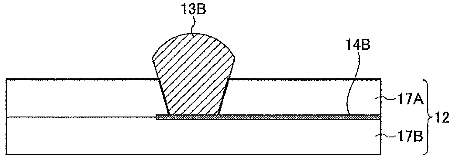
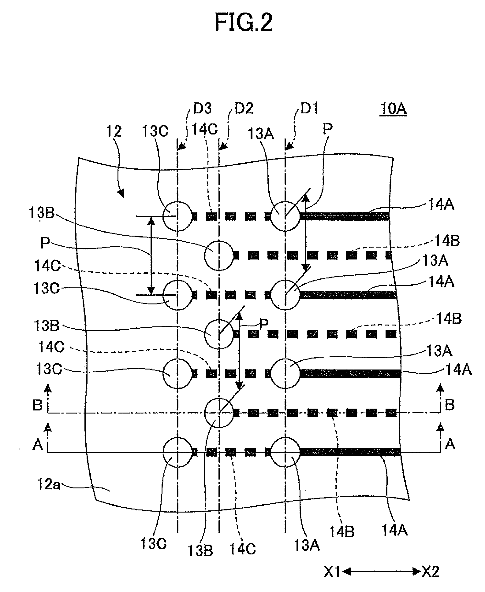
[0016]According to at least one embodiment of the present invention, vias are arranged at the same positions as positions where the bumps are connected on the substrate, and the upper-end portions of the vias are exposed on the surface of the substrate. With this arrangement, the bumps of the electronic device can be directly connected to the upper-end portions of the vias. There is thus no need to form interconnect lines on the surface of the substrate. The inner interconnect lines coupled to the vias can be used to provide electrical coupling for the bumps.
[0017]In such a structure, the inner interconnect lines can be formed on a plurality of layers by use of a multilayer structure substrate. The interconnect lines connected to the bumps through the vias can thus be distributed to the inner interconnect layers, which helps to broaden the pitch of the inner interconnect lines on each layer. This makes it possible to provide the terminals of the electronic device at high density and also to produce the circuit board at low cost while maintaining high electrical characteristics.

Problems solved by technology

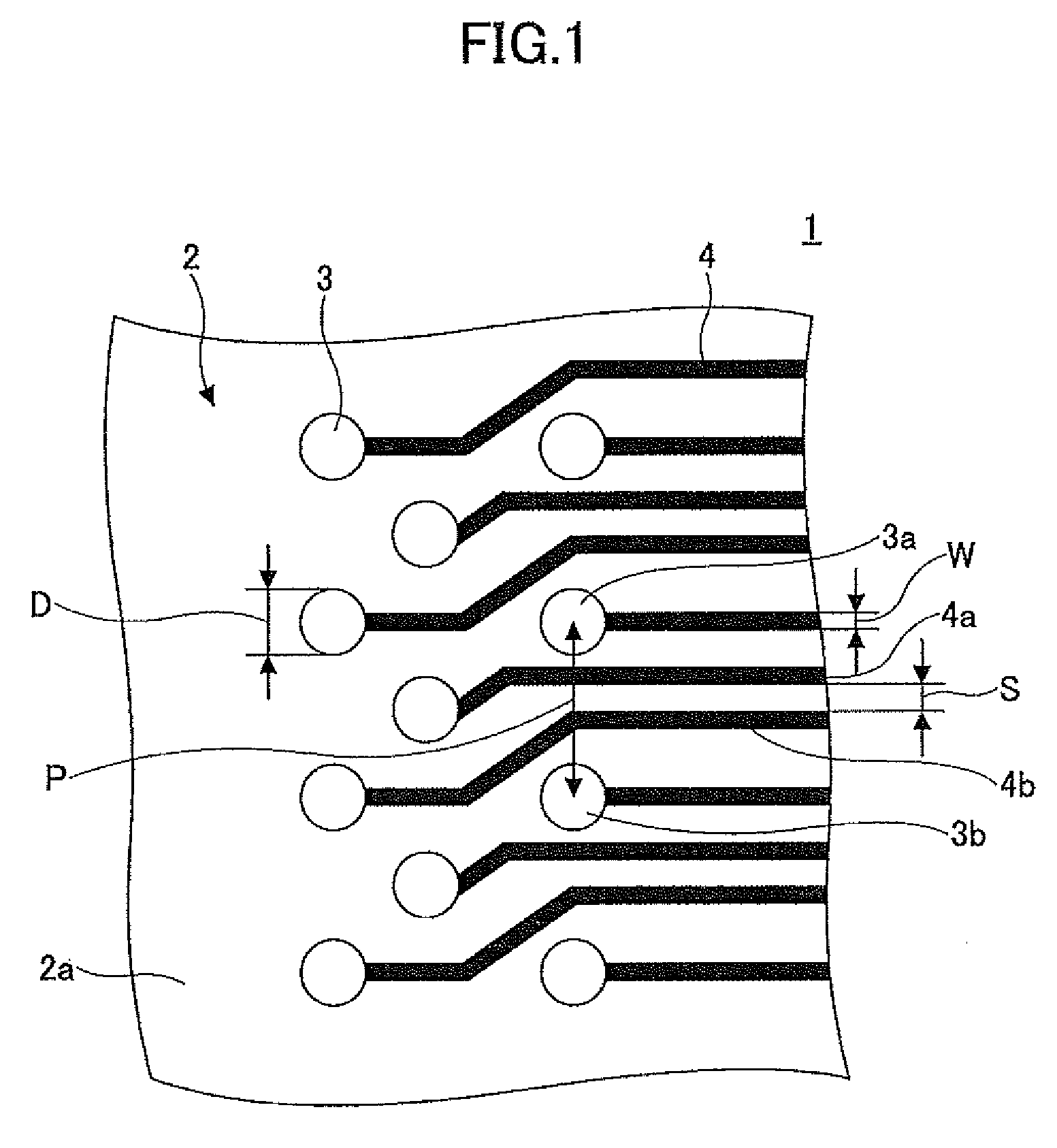
Such high-density wiring requires a more complex fabrication process, causing a drop in yield.
It is almost impossible to use such technology for wire width shorter than 6 μm.
However, an increase in manufacturing cost is a problem.
Further, the use of ceramic as substrate material gives rise to a problem in that parasitic capacitance associated with an increase in dielectric constant may create trouble.

Method used


Image

  • Multilayered Circuit Board for Connection to Bumps
  • Multilayered Circuit Board for Connection to Bumps
  • Multilayered Circuit Board for Connection to Bumps

Examples


Embodiment Construction

[0029]In the following, embodiments for carrying out the present invention will be described by referring to the accompanying drawings.

[0030]FIGS. 2 through 7 illustrate a circuit board 10A according to an embodiment of the present invention. FIG. 2 is a plan view showing an enlarged view of a portion of the circuit board 10A. FIG. 3 and FIG. 4 are drawings showing an interconnect structure and an electronic device when the electronic device is mounted on the circuit board 10A. FIGS. 5 through 7 are plan views of insulating layers constituting the circuit board 10A.

[0031]The circuit board 10A is mainly comprised of a substrate 12 and pad-connection vias 13 (which are individually shown as 13A, 13B, 13C in FIG. 2).

[0032]The substrate 12 has a multilayer structure in which insulating layers and interconnect lines are stacked one over another. The circuit board 10A according to the present embodiment has a three-layer structure in which insulating layers 17A through 17C and interconnec...


PUM


Abstract

A circuit board on which an electronic device having bumps arranged in an array form is to be mounted includes a substrate having a multilayer structure that includes interconnect lines and insulating layers, and vias penetrating through one or more of the insulating layers and coupled to one or more of the interconnect lines, wherein the vias are arranged at positions that are the same as positions of the bumps to be connected on the substrate, and the vias project from a surface of the substrate so that upper-end portions of the vias are exposed from the surface of the substrate.

Description

BACKGROUND OF THE INVENTION[0001]1. Field of the Invention[0002]The disclosures herein generally relate to circuit boards, interconnect structures, and electronic devices, and particularly relate to a circuit board, an interconnect structure, and an electronic apparatus suitable for high circuit density.[0003]2. Description of the Related Art[0004]As the functionality and circuit density of electronic devices increase, the number of terminals of an electronic device (i.e., the number of flip-chip I / Os) increases, and, also, a bump pitch narrows. This gives rise to a need to provide high-density wiring for interconnection to bumps in the circuit substrate on which an electronic device is mounted. Such high-density wiring requires a more complex fabrication process, causing a drop in yield. In consideration of this, various studies have been conducted with respect to circuit boards having wiring structures suitable for an electronic device having high circuit density (see Japanese Pat...

Claims


Application Information

Patent Timeline
Patent Type & Authority Applications(United States)
IPC IPC(8): H01R12/02H01R12/50
CPCH01L21/4853H01L2224/16235H01L23/49822H01L23/49827H01L23/49838H01L24/17H01L2224/13099H01L2224/16H01L2924/01015H01L2924/01029H01L2924/01074H01L2924/01078H01L2924/15174H01L2924/30105H05K1/113H05K2201/0367H05K2201/09227H05K2201/09436H05K2201/10674H01R12/714H01L2924/01005H01L2924/01006H01L2924/01033H01L2924/01076H01L23/49816
Inventor HORIUCHI, MICHIOTOKUTAKE, YASUESUGANUMA, SHIGEAKIKOIZUMI, NAOYUKIKATAGIRI, FUMIMASA
Owner SHINKO ELECTRIC IND CO LTD
Why Eureka
Eureka Blog
Learn More