Semiconductor device and method of manufacturing semiconductor device

a semiconductor device and semiconductor technology, applied in semiconductor devices, semiconductor/solid-state device details, electrical devices, etc., can solve the problem that the second electronic component b>203/b> cannot be fixedly mounted, and achieve the effect of reducing the thickness of the semiconductor devi

Inactive Publication Date: 2010-08-26
SHINKO ELECTRIC IND CO LTD
View PDF17 Cites 11 Cited by
  • Summary
  • Abstract
  • Description
  • Claims
  • Application Information

AI Technical Summary

Benefits of technology

[0016]According to at least one embodiment, the size of the semiconductor device in the thickness direction is reduced. Further, a second electronic component having a larger surface size than the first electronic component may be fixedly mounted to the first electronic component in a stable manner.

Problems solved by technology

This gives rise to a problem in that the second electronic component 203 may not be fixedly mounted on the first electronic component 202 in a stable manner.

Method used


Image

  • Semiconductor device and method of manufacturing semiconductor device
  • Semiconductor device and method of manufacturing semiconductor device
  • Semiconductor device and method of manufacturing semiconductor device

Examples


first embodiment

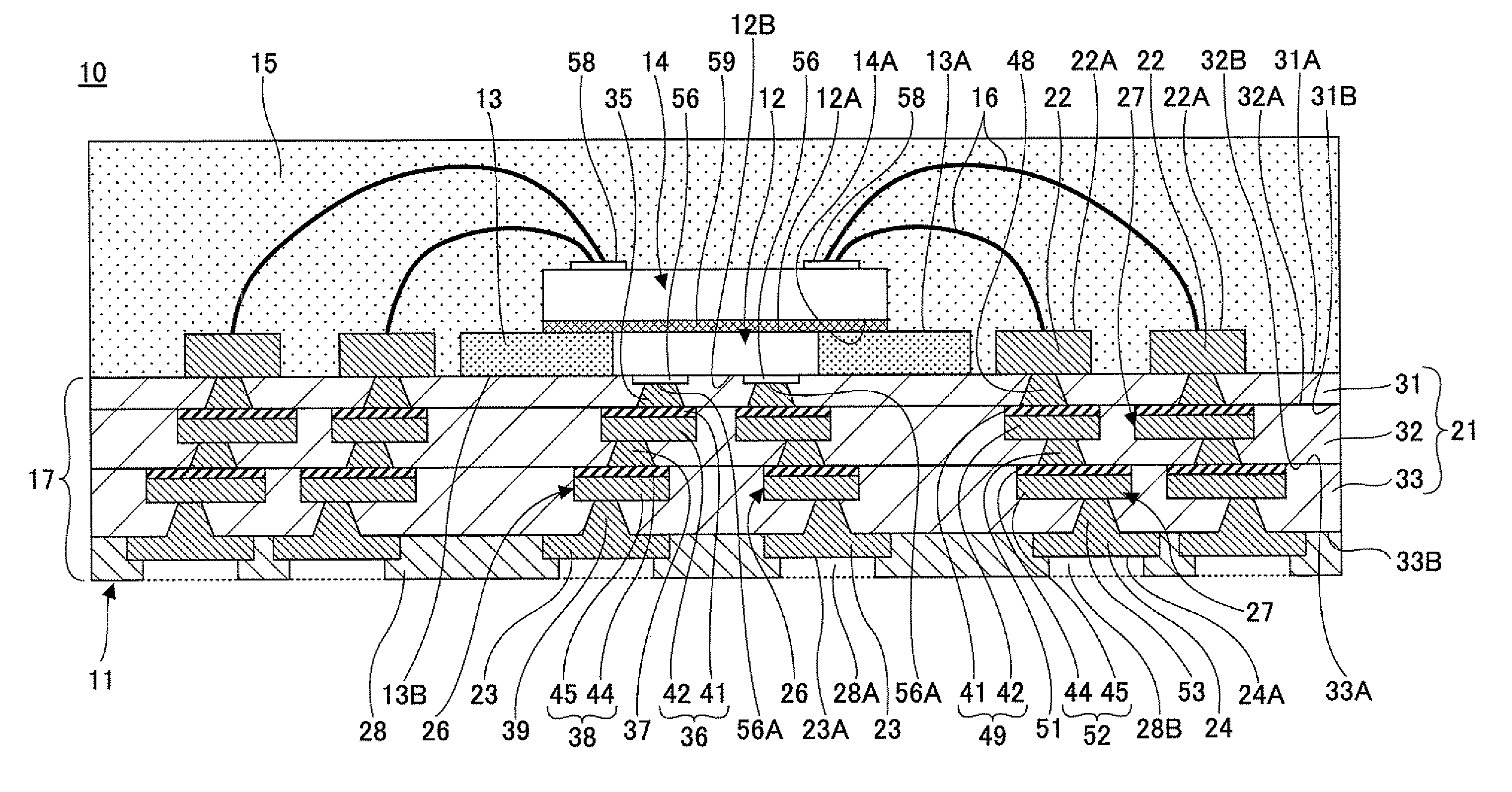
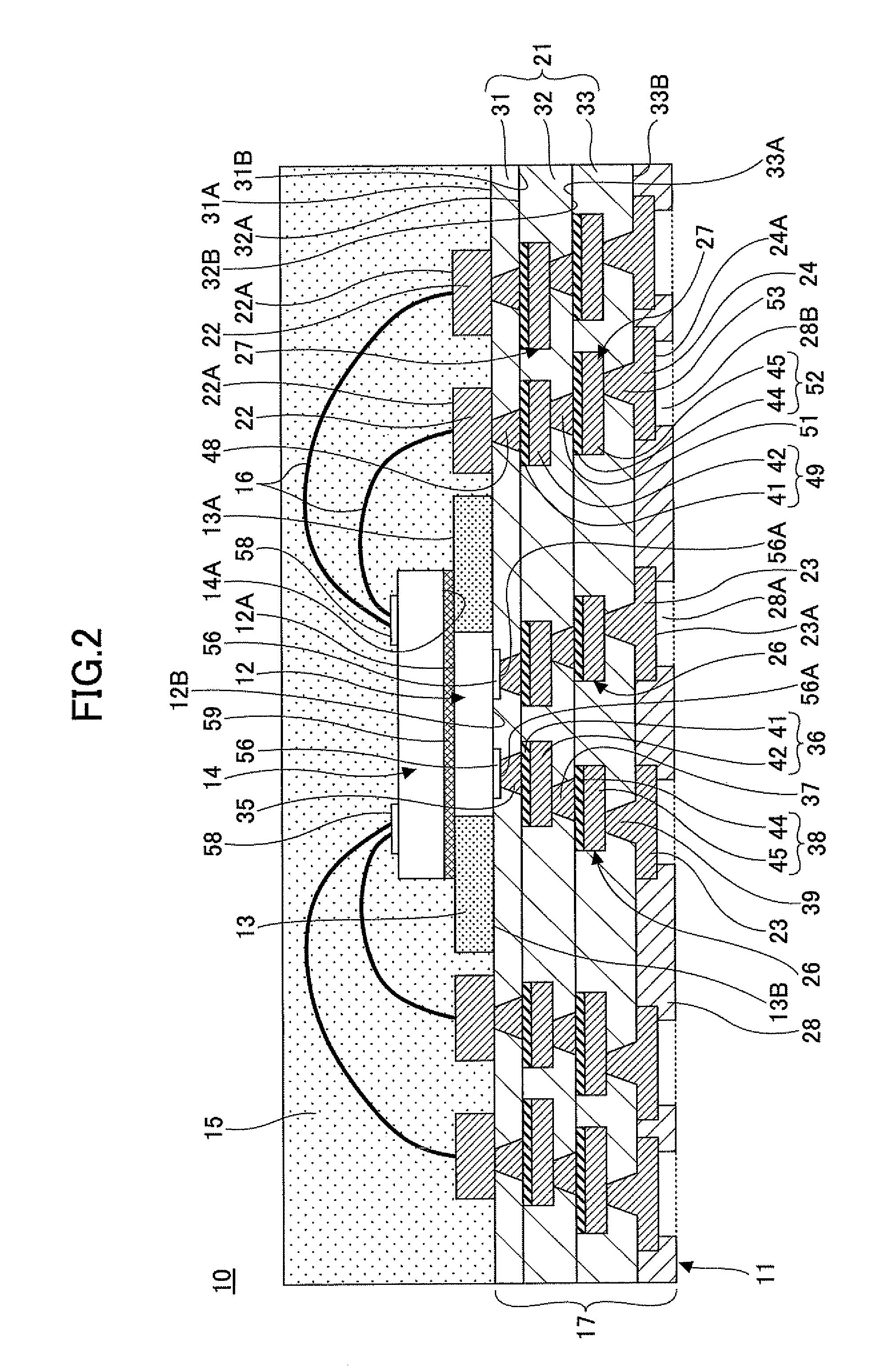
[0046]FIG. 2 is a cross-sectional view of a semiconductor device according to a first embodiment.

[0047]A semiconductor device 10 illustrated in FIG. 2 includes a wiring substrate 11, a first electronic component 12, sealing resins 13 and 15, and a second electronic component 14.

[0048]The wiring substrate 11 includes a multilayer interconnection structure 17 and pads 22. The multilayer interconnection structure 17 includes a multilayer structure 21, first external connection pads 23, second external connection pads 24, first interconnection patterns 26, second interconnection patterns 27, and a solder resist layer 28. The first interconnection patterns 26 and the second interconnection patterns 27 may be connected to each other in the multilayer interconnection structure 17.

[0049]The multilayer structure 21 is situated to face the lower surface (i.e., first surface) of the sealing resin 13, electrode pads 56 formed on the electronic component 12, and an electrode pad forming surface ...

second embodiment

[0148]FIG. 25 is a cross-sectional view of a semiconductor device according to a second embodiment. In FIG. 25, the same elements as those of the semiconductor device 10 of the first embodiment are referred to by the same numerals.

[0149]A semiconductor device 100 of the second embodiment illustrated in FIG. 25 has the same configuration as the semiconductor device 10 of the first embodiment, except that a plurality of first electronic components 12 are provided.

[0150]The first electronic components 12 are situated on the upper surface 31A of the insulating layer 31. The electrode pads 56 of the first electronic components 12 are directly connected to the top ends of the vias 35.

[0151]The sealing resin 13 is disposed on the sides of the first electronic components 12 and between the first electronic components 12. The upper surface 13A of the sealing resin 13 is configured to be substantially flush with the back surfaces 12A of the first electronic components 12.

[0152]The second elec...


PUM


Abstract

A semiconductor device includes an electronic component having a pad surface on which an electrode pad is formed, and having a back surface opposite the pad surface, a sealing resin disposed to cover side faces of the electronic component while exposing the pad surface at a first surface thereof and the back surface at a second surface thereof, a multilayer interconnection structure including insulating layers stacked one over another and interconnection patterns, having an upper surface thereof being in contact with the first surface, the electrode pad, and the pad surface, and having a periphery thereof situated outside a periphery of the sealing resin, and another pad disposed on the upper surface of the multilayer interconnection structure outside the periphery of the sealing resin, wherein the interconnection patterns include a first interconnection pattern directly connected to the electrode pad and a second interconnection pattern directly connected to said another pad.

Description

BACKGROUND OF THE INVENTION[0001]1. Field of the Invention[0002]The disclosures herein generally relate to semiconductor devices and methods of manufacturing semiconductor devices, and particularly relate to a semiconductor device and a method of manufacturing a semiconductor device that includes a wiring substrate and electronic components mounted on the wiring substrate.[0003]2. Description of the Related Art[0004]A certain type of semiconductor device achieves high-density implementation of electronic components by stacking the electronic components in a multilayer structure on a wiring substrate.[0005]FIG. 1 is a cross-sectional view of a related-art semiconductor device. A semiconductor device 200 illustrated in FIG. 1 includes a wiring substrate 201, a first electronic component 202, and a second electronic component 203. The wiring substrate 201 includes a substrate 211, pads 213 and 214, and external connection pads 215.[0006]The substrate 211 includes a plurality of insulat...

Claims


Application Information

Patent Timeline
Patent Type & Authority Applications(United States)
IPC IPC(8): H01L23/522H01L21/60
CPCH01L21/6835H01L23/3121H01L23/49822H01L23/5389H01L24/16H01L24/24H01L24/45H01L24/48H01L25/0652H01L25/0657H01L25/18H01L2221/68345H01L2224/04105H01L2224/16225H01L2224/16237H01L2224/20H01L2224/24227H01L2224/32145H01L2224/45144H01L2224/48091H01L2224/48227H01L2224/48235H01L2224/73265H01L2224/83101H01L2225/0651H01L2225/06517H01L2225/06524H01L2924/01004H01L2924/01014H01L2924/01029H01L2924/01078H01L2924/01079H01L2924/15153H01L2924/1517H01L2924/15174H01L2924/01006H01L2924/01033H01L2224/32225H01L24/83H01L2924/01028H01L24/19H01L2224/0401H01L2224/16235H01L2924/00014H01L2924/00H01L2924/00012H01L2924/181H01L24/73H01L2224/73267
Inventor SHIMIZU, NORIYOSHI
Owner SHINKO ELECTRIC IND CO LTD
Why Eureka
Try Eureka