Radio frequency indentification tag

a technology of indentification and radio frequency, applied in the field of communication technique of radio frequency identification system, can solve the problems of inability to supply the rectification circuit, power input to the rectification circuit, etc., and achieve the effect of sufficient back scattering strength, improving communication quality, and expanding the range allowing communication

Inactive Publication Date: 2009-05-28
RENESAS ELECTRONICS CORP
View PDF6 Cites 57 Cited by
  • Summary
  • Abstract
  • Description
  • Claims
  • Application Information

AI Technical Summary

Benefits of technology

[0018]Furthermore, if the distance between the ID tag and the reader / writer in communication is very short, the receiving power at the ID tag becomes large and a large voltage is applied to the elements of the rectification circuit. To assure the voltage proofness of the elements of the rectification circuit, a protection circuit is generally added to the rectification circuit. The protection circuit withdraws current only in case of large power input to the rectification circuit and decreases the potentials of the elements of the rectification circuit.
[0020]An object of the present invention is to provide a technique that enables a stable supply of an internal supply voltage and extending the ID tag communication range during back scattering communication.
[0033](1) It is possible to extend the range allowing communication between the ID tag and the reader / writer during back scattering communication.
[0034](2) It is possible to attain a sufficient strength of back scattering even if the receiving power is large in very short distance communication.
[0035](3) It is possible to improve the quality of communication carried out in an RFID system, owing to the advantages set forth in (1) and (2).

Problems solved by technology

However, the inventors have found that the above-described communication technique by means of backscattering for RFID systems has the following problems.
However, during back scattering communication, the antenna terminals are short-circuited by the switch for back scattering short circuits and, therefore, this shuts off the input of power to the rectification circuit following the antenna.
This poses a problem that the rectification circuit becomes unable to supply current to the internal circuit during back scattering communication.

Method used


Image

  • Radio frequency indentification tag
  • Radio frequency indentification tag
  • Radio frequency indentification tag

Examples


first embodiment

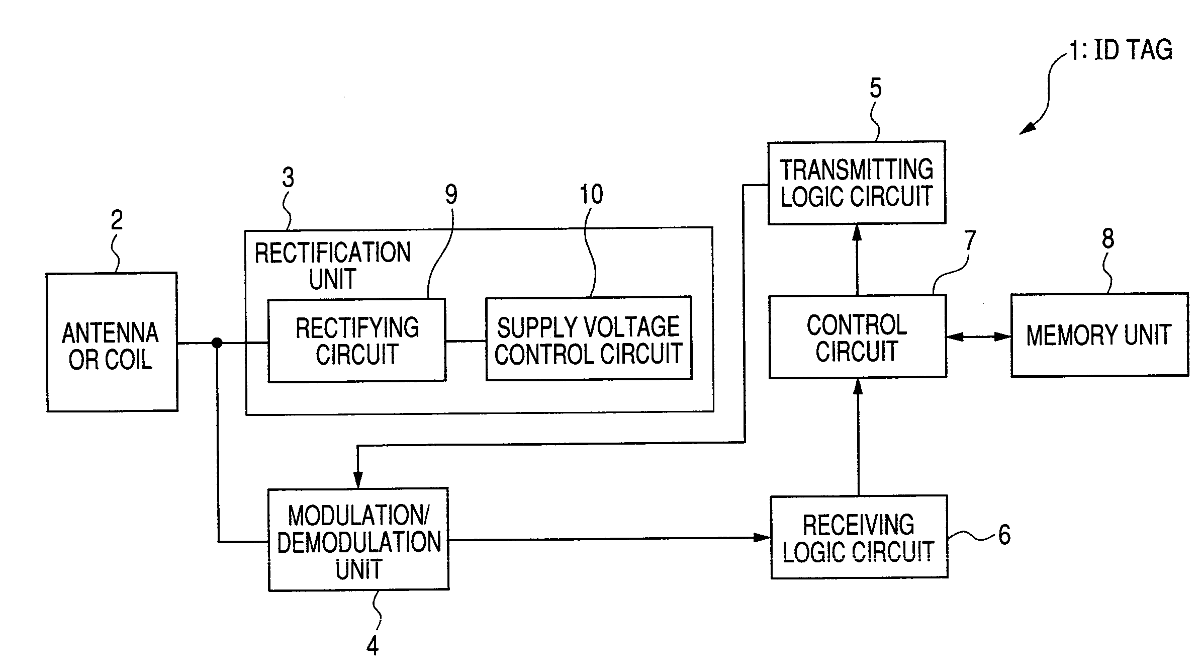
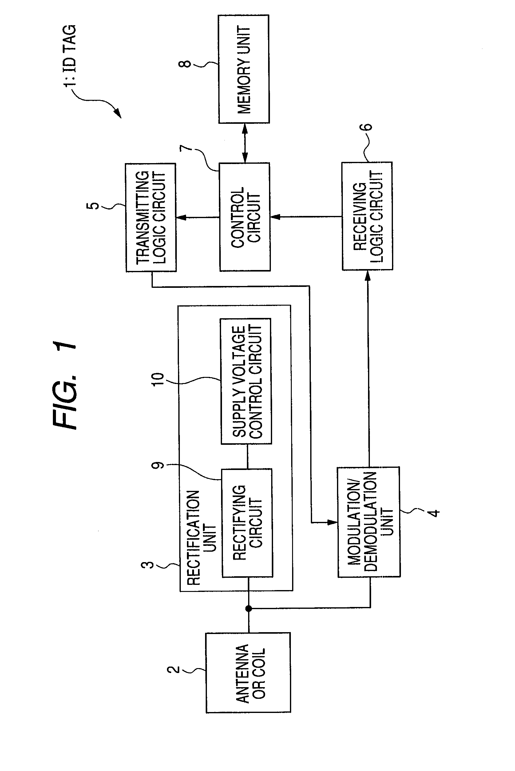
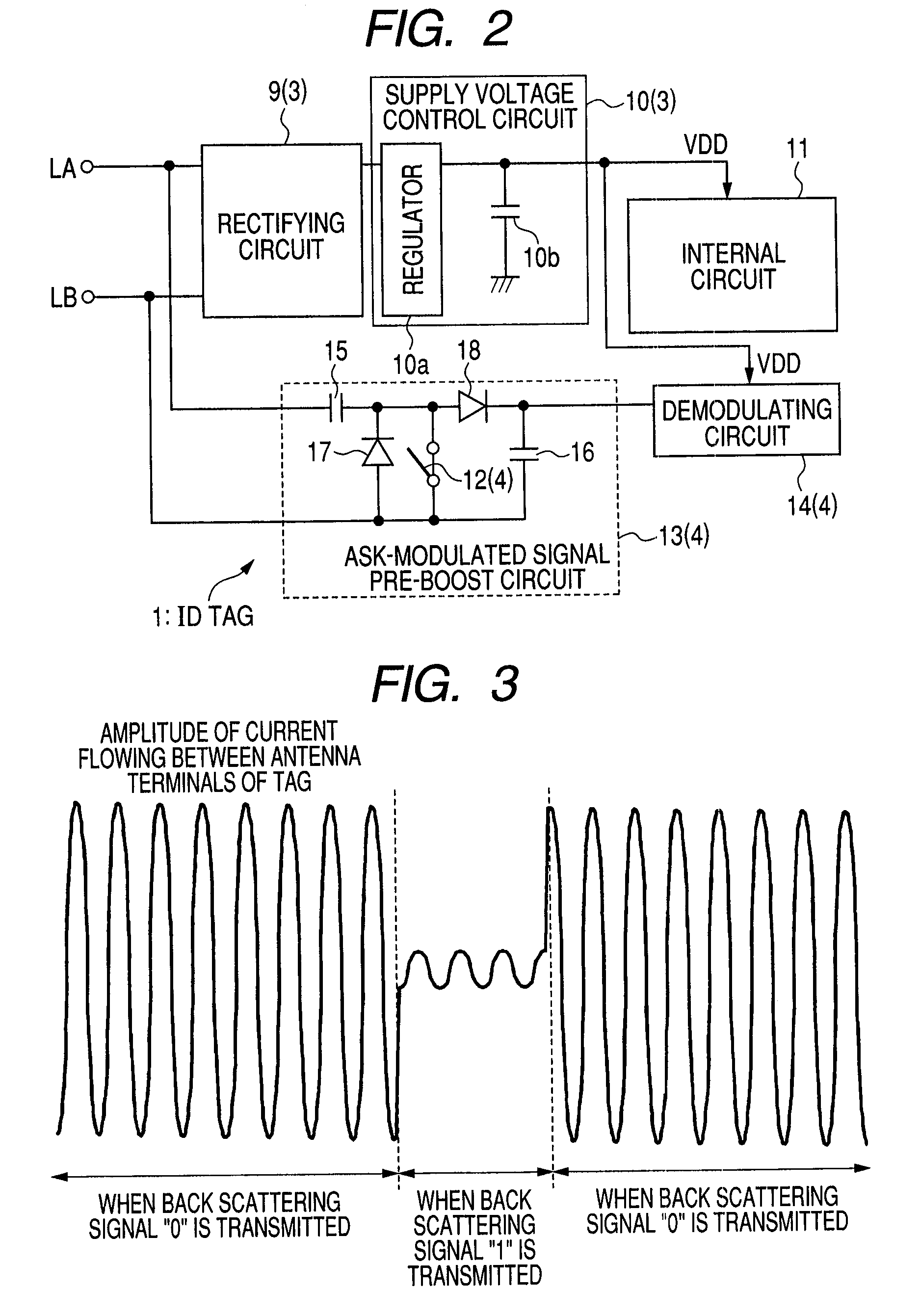
[0046]FIG. 1 is a block diagram showing an ID tag configuration according to a first embodiment of the present invention. FIG. 2 is a diagram illustrating an example of a configuration for a rectification unit and a modulation / demodulation unit in the ID tag of FIG. 1. FIG. 3 is a diagram for a back scattering signal transmitted by the ID tag during back scattering communication.

[0047]In the first embodiment, the ID tag 1 is used for RFID, an automatic identification technique. The ID tag 1, as shown in FIG. 1, is comprised of an antenna 2, a rectification unit 3, a modulation / demodulation unit 4, a transmitting logic circuit 5, a receiving logic circuit 6, a control circuit 7, and a memory unit 8.

[0048]The rectification unit 3 generates an internal supply voltage VDD that is used as the operating power from radio waves received by the antenna 2. The rectification unit 3 supplies the VDD to the modulation / demodulation unit 4, transmitting logic circuit 5, the receiving logic circuit...

second embodiment

[0074]FIG. 4 is a diagram illustrating an example of circuitry including an ASK-modulated signal pre-boost circuit and a switch for back scattering provided in an ID tag according to a second embodiment of the present invention. FIG. 5 is a circuit diagram showing a configuration example for a rectification unit and a modulation / demodulation unit shown in FIG. 4.

[0075]In the second embodiment, the ID tag 1 (FIG. 1) is comprised of an antenna 2, a rectification unit 3, a modulation / demodulation unit 4, a transmitting logic circuit 5, a receiving logic circuit 6, a control circuit 7, and a memory unit 8 in the same way as the foregoing first embodiment.

[0076]The rectification unit 3 is comprised of a rectifying circuit 9, a regulator 10a, and a static capacitor 10b, as is the case for the foregoing first embodiment. The modulation / demodulation unit 4 is comprised of a switch 12 for back scattering (modulator element) and a demodulator comprising an ASK-modulated signal pre-boost circu...

third embodiment

[0093]FIG. 6 is a diagram illustrating a configuration for a rectification unit, a modulation / demodulation unit, a memory unit, a boost circuit for memory, and an internal circuit provided in an ID tag according to a third embodiment of the present invention.

[0094]In the third embodiment, the ID tag 1 comprises an antenna 2, a rectification unit 3, a modulation / demodulation unit 4, a transmitting logic circuit 5, a receiving logic circuit 6, a control circuit 7, and a memory unit 8 in the same configuration as for the above first embodiment, and further includes a boost circuit for memory 8a for supplying power to the memory unit 8.

[0095]FIG. 6 is a diagram illustrating the configuration for the rectification unit 3, modulation / demodulation unit 4, memory unit 8, and boost circuit for memory in the ID tag 1.

[0096]In this case, the switch 12 for back scattering is provided in the boost circuit for memory 8a, which is different from the above first embodiment, instead of being provide...


PUM


Abstract

The disclosed ID tag has a stable internal supply voltage and extends the range of communication with the reader / writer during back scattering communication. An ASK-modulated signal pre-boost circuit to which antenna terminals are coupled is coupled in parallel with a rectifying circuit. In the ASK-modulated signal pre-boost circuit, a switch for back scattering, working as a modulator element, is provided. During back scattering communication, when a back scattering signal “1” is transmitted, only the current flowing in the signal receiving path of the modulation / demodulation unit is wasted by turning the switch for back scattering on. Additional current loss other than the loss for impedance matching can be prevented.

Description

CROSS-REFERENCE TO RELATED APPLICATIONS [0001]The disclosure of Japanese Patent Application No. 2007-307000 filed on Nov. 28, 2007 including the specification, drawings and abstract is incorporated herein by reference in its entirety.BACKGROUND OF THE INVENTION[0002]The present invention relates to a communication technique for RFID (Radio Frequency Identification) systems and, particularly, to a technique that is effective for improving the quality of communication for transferring data from / to an ID tag (identification tag).[0003]RFID is disseminating as an automatic identification technique in which data can be transferred by wireless communication. An RFID system comprises an ID tag capable of storing information and a read / writer that performs reading and writing information from / to the ID tag. An ID tag comprises a semiconductor integrated circuit device such as, e.g., a non-contact IC chip, and an antenna.[0004]The ID tag receives radio waves output from the read / writer and a...

Claims


Application Information

Patent Timeline
Patent Type & Authority Applications(United States)
IPC IPC(8): H04Q5/22
CPCG06K19/0713G06K19/0723H04B5/0031H04Q2213/13095H04B5/0062H04B5/02H04B5/0037
Inventor TSUKAMOTO, TAKAYUKIMOTOJIMA, MUTSUYA
Owner RENESAS ELECTRONICS CORP
Why Eureka
Try Eureka