
Eureka
For R&D, Eureka makes reading and utilizing patents & technical documents easy.
Eureka AIR
Designed for self-driven R&D workflows. Generate viable solutions, solve complex R&D challenges, empower your innovation with AI.

Eureka Materials
Designed for material experts only. Revolutionize your material R&D, from search, analyze, to developing new materials.

TechResearch
Generate reliable direction feasibility study reports for your R&D in just a few steps.

TechSeek
Discover and master advanced knowledge NOW. Basics, ideas, possibilities, all at once.

TechMind
As an expert in R&D Theories, TechMind can generates customized viable solutions instantly.

TechRisk
Analyze your overall solution with one click, know your potential R&D risks in advance.

TechMonitor
Get weekly tech updates, stay abreast of the latest tech innovations and key insights.
Semiconductor apparatus
- Summary
- Abstract
- Description
- Claims
- Application Information
AI Technical Summary
Benefits of technology
Problems solved by technology
Method used
Image

Examples
first embodiment
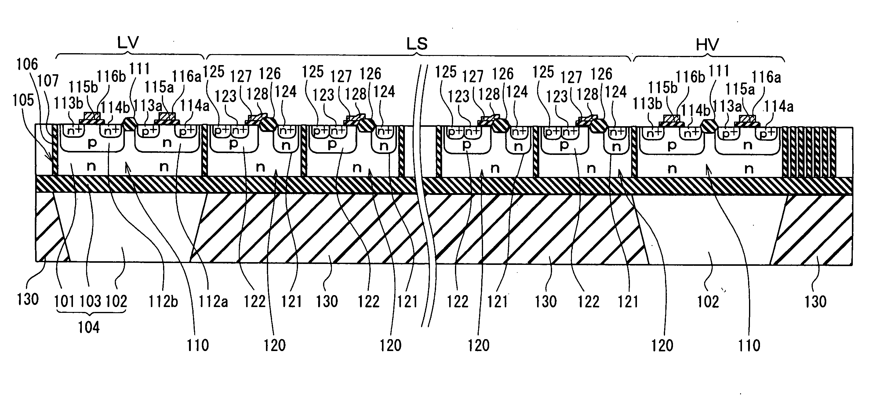
[0045]A configuration of a semiconductor apparatus of a first embodiment is described below with reference to FIGS. 1 to 3. In the following description, it is assumed that a front surface side of a semiconductor apparatus corresponds to one described in an upper side of FIG. 1, and a rear surface side of the semiconductor apparatus corresponds to one described in a lower side of FIG. 1.
[0046]As shown in FIG. 1, the semiconductor apparatus is formed by using a silicon on insulator SOI substrate 104, which includes a support substrate 102 and an SOI layer 101 bonded through a buried oxide film 103. The SOI layer 101 is made of, for example, P type silicon. The SOI layer 101 functions as an active layer 101. The buried oxide film 103 functions as a buried insulation film 103.
[0047]The SOI layer 101 is located on the front surface side of the semiconductor apparatus and is formed by grinding a silicon substrate to a predetermined thickness. In the SOI layer 101, multiple trench isolati...
second embodiment
[0065]A difference between a semiconductor apparatus of the present embodiment and that of a first embodiment includes a configuration for setting a potential of the support substrate 102.
[0066]FIG. 6 is a cross sectional diagram illustrating a semiconductor apparatus (i.e., HVIC) in accordance with the present embodiment. As shown in FIG. 6, the semiconductor apparatus has a second terminal (not shown) for receiving the reference potential of the high potential reference circuit part HV. The second terminal and the second portion of the support substrate 102 are electrically connected with each other so as to have a substantially same potential. The second portion of the support substrate 102 is located at a place corresponding to the high potential reference circuit part HV, or in other words, the second portion is located opposite to the high potential reference circuit part HV with respect to the buried oxide film 103. More specifically, a base 141 having a conductive pattern 14...
third embodiment
[0074]A difference between a semiconductor apparatus of the present embodiment and that of a first embodiment includes arrangement of the support substrate 102. In the present embodiment, the support substrate 102 has a third portion, which is located on a place corresponding to an element-outside part.
[0075]FIG. 9 is a cross sectional diagram taken along line IX-IX in FIG. 10 and illustrating a semiconductor apparatus in accordance with the present embodiment. FIG. 10 is a diagram illustrating a layout of elements on a rear surface side of the semiconductor apparatus illustrated in FIG. 9.
[0076]As shown in FIGS. 9 and 10, an element-outside part 150 is located outward of the outermost trench insulation member 105. A third portion of the support substrate 102 is located at a place that corresponds to the element-outside part 150. The third portion of the support substrate 102 is opposite to the element-outside part 150 with respect to the buried oxide film 103. More specifically, th...
PUM
 Abstract
Description
Claims
Application Information
 - R&D Engineer
- R&D Manager
- IP Professional
- Industry Leading Data Capabilities
- Powerful AI technology
- Patent DNA Extraction
Browse by: Latest US Patents, China's latest patents, Technical Efficacy Thesaurus, Application Domain, Technology Topic, Popular Technical Reports.
© 2024 PatSnap. All rights reserved.Legal|Privacy policy|Modern Slavery Act Transparency Statement|Sitemap|About US| Contact US: help@patsnap.com