Semiconductor module mounting structure

Inactive Publication Date: 2009-06-25
DENSO CORP
View PDF4 Cites 13 Cited by
  • Summary
  • Abstract
  • Description
  • Claims
  • Application Information

AI Technical Summary

Benefits of technology

[0015]According to the present invention, there is provided a semiconductor module mounting stru

Problems solved by technology

However, since the surface on the side opposite to the heat radiating plate is covered by the resin material, it is difficult to dissipate heat through this surface.
Accordingly, it is difficult to sufficiently dissipate heat transmitte

Method used


Image

  • Semiconductor module mounting structure
  • Semiconductor module mounting structure
  • Semiconductor module mounting structure

Examples


Example

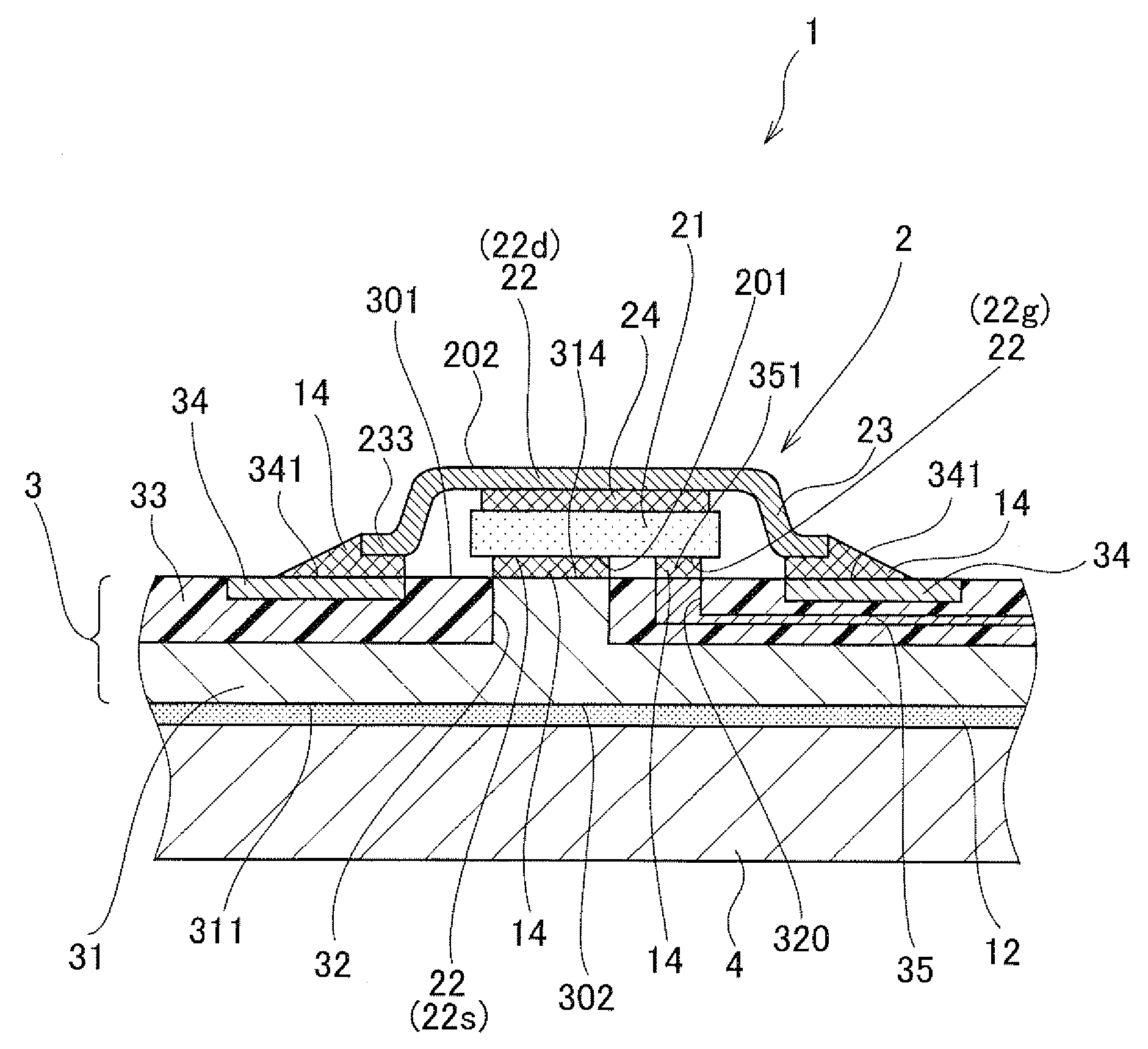
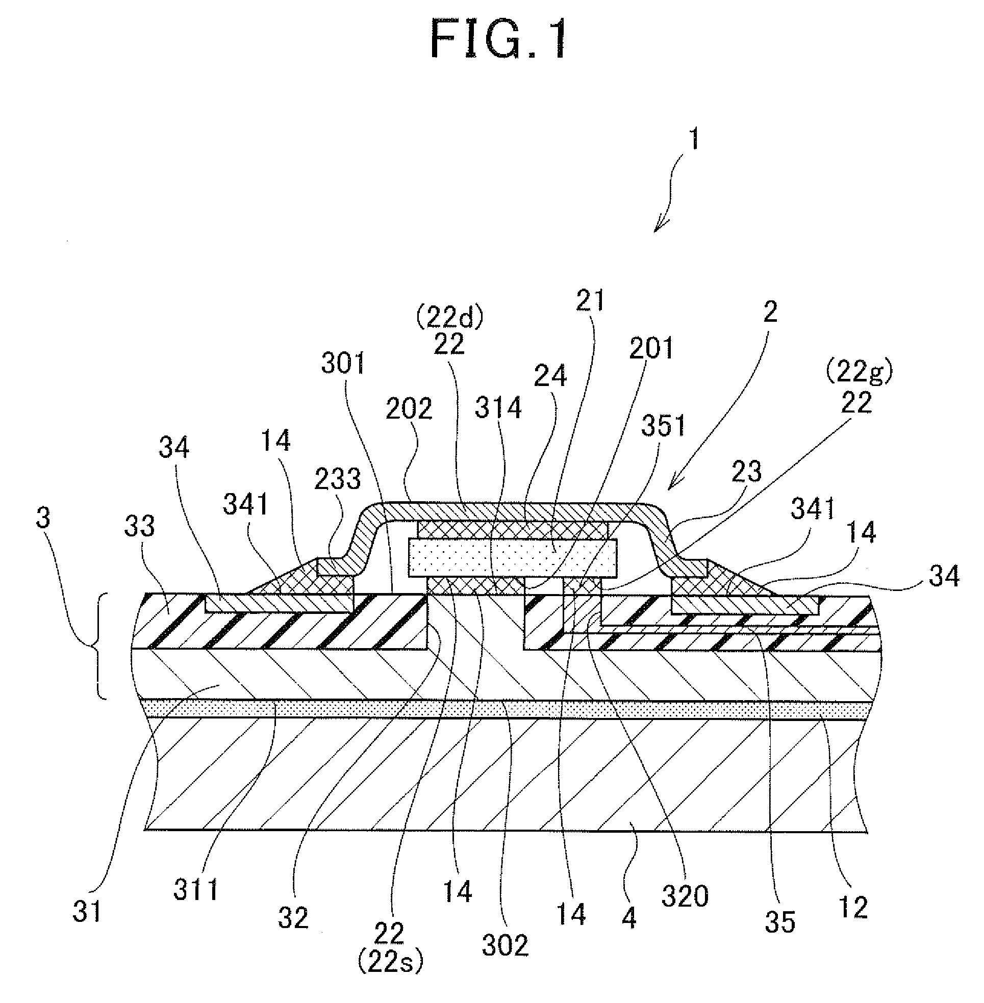
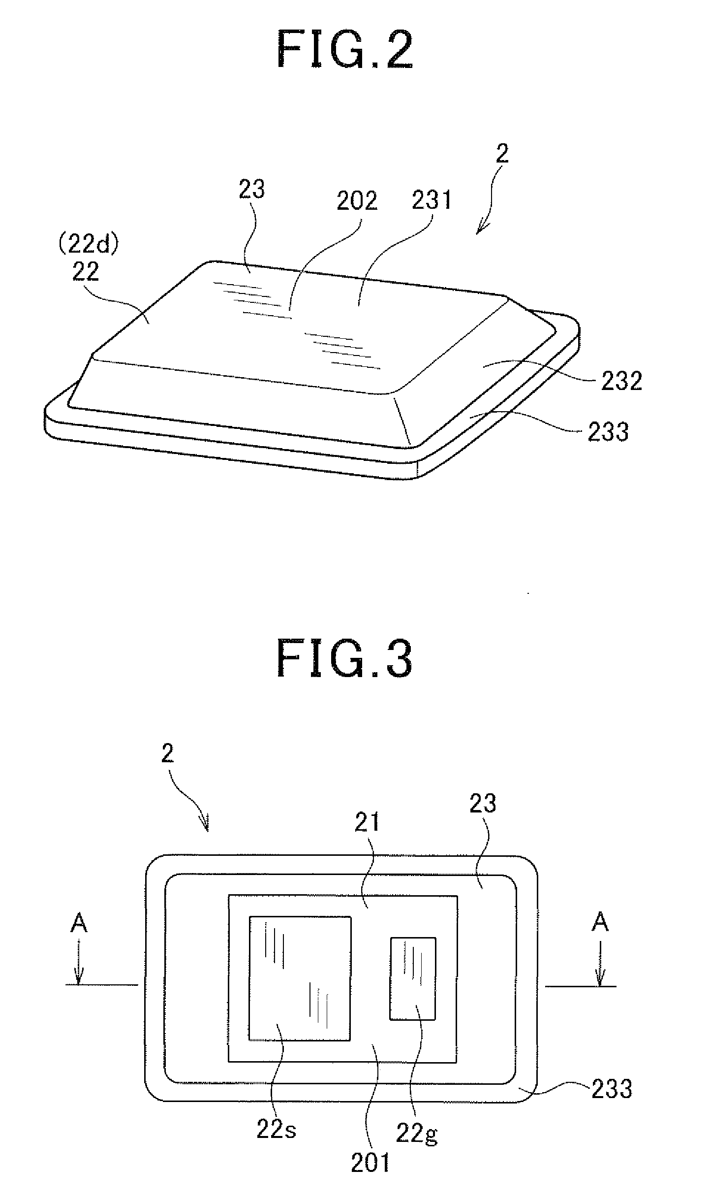
[0033]A semiconductor module mounting structure 1 of a first embodiment of the invention is described with reference to FIGS. 1 to 7. As shown in FIGS. 1 to 4, the semiconductor module mounting structure 1 of this embodiment has a structure in which a semiconductor module 2 including therein a semiconductor device 21, and electrodes 22 exposed to both surfaces in the thickness direction thereof is mounted on a wiring substrate 3.

[0034]As shown in FIG. 1 and FIG. 6B, the wiring substrate 3 has a structure in which a ground wiring 31 is laid so as to be exposed at least partially to a back surface 302 of the wiring substrate 3 opposite to a front mounting surface 301 of the wiring substrate 3 on which the semiconductor module 2 is mounted. As shown in FIG. 1, an exposed surface 311 of the ground wiring 31 exposed to the back surface 302 is thermally connected to a heat radiating body 4.

[0035]The semiconductor module 2 connects the electrode 22s exposed to an opposed surface 201 thereo...

Example

Second Embodiment

[0054]As shown in FIGS. 8 and 9, the second embodiment of the invention is characterized in that the first wiring pattern 34 and the second wiring pattern 35 are formed on the mounting surface 301, and the wiring substrate 3 is formed of a film-like insulating substrate having the through hole 32 formed therein. The wiring substrate 3 is adhered to the surface of the conductive plate 310, and a conductor 321 within the through hole 32 is connected to the conductive plate 310.

[0055]The film-like insulating substrate 33 is joined to the conductive plate 310 by a prepreg, and the conductor 321 within the through hole 32 is connected to the conductive plate 310 by solder or conductive paste. The film-like insulating substrate 33 has a thickness of 0.2 to 0.5 mm.

[0056]The first wiring pattern 34 connected to the drain terminal (electrode 22d), and the second wiring pattern 35 connected to the gate terminal (electrode 22g) are formed on the mounting surface 301. As shown ...

Example

Third Embodiment

[0058]The third embodiment of the invention shown in FIG. 10 is characterized in that the electrode 22d exposed to the back surface 202 of the semiconductor module 2 is disposed so as to be in thermal contact with a backside heat radiating body 40. The backside heat radiating body 40, which is made of aluminum or its alloy, is provided with heat-radiating fins 41 at its surface opposite to its other surface contacting the backside surface 202 of the semiconductor module 2. The other components of this embodiment are the same as those of the second embodiment.

[0059]Also according to this embodiment, the semiconductor module mounting structure capable of dissipating heat further efficiently can be obtained, because heat can be dissipated efficiently also from the electrode 22d exposed to the back surface 202 of the semiconductor module 2. The third embodiment provides, in addition to the above advantage, the same advantages as provided by the second embodiment.


PUM


Abstract

The semiconductor module mounting structure includes a semiconductor module including therein a semiconductor device and electrodes exposed to both surfaces thereof, a wiring substrate having a mounting surface on which the semiconductor module is mounted, and a heat radiating body for dissipating heat from the semiconductor module. The wiring substrate is formed with a ground wiring such that at least a part of the ground wiring is exposed to a back surface thereof opposite to the mounting surface. The exposed surface of the ground wiring exposed to the back surface is in thermal contact with the heat radiating body. At least one of the electrodes exposed to one of the both surfaces opposed to the wiring substrate is in electrical contact with the ground wiring through a through hole formed in the wiring substrate.

Description

CROSS-REFERENCE TO RELATED APPLICATION[0001]This application is related to Japanese Patent Application No. 2007-331241 filed on Dec. 24, 2007, the contents of which are hereby incorporated by reference.BACKGROUND OF THE INVENTION[0002]1. Field of the Invention[0003]The present invention relates to a semiconductor module mounting structure in which a semiconductor module including therein a semiconductor device and having electrodes exposed to both surfaces in the thickness direction thereof is mounted on a wiring substrate.[0004]2. Description of Related Art[0005]It is known to use, as switching elements of a power conversion device such as an inverter, semiconductor devices such as MOSFETs. Such a semiconductor device may be mounted on the power conversion device in the form of a semiconductor module having a structure in which electrodes located at one surface of the semiconductor module are solder-joined to a heat radiating plate, and the semiconductor device is encapsulated by a...

Claims


Application Information

Patent Timeline
IPC IPC(8): H01L23/04H01L23/48H01L23/34H01L23/14
CPCH01L23/04H01L23/3677H01L2924/1305H01L2924/1306H01L2924/014H01L2924/10253H01L2924/01033H01L2924/01023H01L2924/01006H01L2924/19043H01L2924/19041H01L23/40H01L23/433H01L23/492H01L23/49844H01L24/16H01L24/28H01L24/33H01L24/35H01L24/36H01L24/40H01L24/73H01L2224/13099H01L2224/73153H01L2224/73253H01L2924/01005H01L2924/01013H01L2924/01015H01L2924/01027H01L2924/01029H01L2924/01047H01L2924/01058H01L2924/01074H01L2924/01078H01L2924/01082H01L2924/13055H01L2924/13091H01L2924/16152H01L2924/00H01L2224/40225H01L2224/05573H01L2224/05568H01L2924/00014H01L2224/84801H01L2224/37147H01L2224/83801H01L24/37H01L2224/371H01L2224/37599H01L24/06H01L24/05H01L2224/0603H01L2224/06181H01L24/84H01L2224/05599
Inventor TANIGUCHI, MAKOTOKABUNE, HIDEKITANAKA, KATSUNORITANAKA, YUKARI
Owner DENSO CORP
Why Eureka
Try Eureka