Solid-state imaging device, method of manufacturing the same, and camera and electronic apparatus using the same

Inactive Publication Date: 2009-07-02
SONY CORP
View PDF1 Cites 36 Cited by
  • Summary
  • Abstract
  • Description
  • Claims
  • Application Information

AI Technical Summary

Benefits of technology

[0033]The camera or the electronic apparatus having such a camera according to an embodiment of the present invention uses the solid-state imaging device with a reduced difference in level on the boundary between the effective pixel region and the peripheral area.
[0034]Acc

Problems solved by technology

However, it is difficult to planarize the surface by the CMP method.
Therefore, if there is a difference in level on the surface of the buried layer or a difference in film thickness thereof on the boundaries between the effective pixel region, the optical black region, and the peripheral circuit region of the solid-state imaging device, such a difference may affect any layer on or above the buried layer.
As a result, th

Method used


Image

  • Solid-state imaging device, method of manufacturing the same, and camera and electronic apparatus using the same
  • Solid-state imaging device, method of manufacturing the same, and camera and electronic apparatus using the same
  • Solid-state imaging device, method of manufacturing the same, and camera and electronic apparatus using the same

Examples


first example

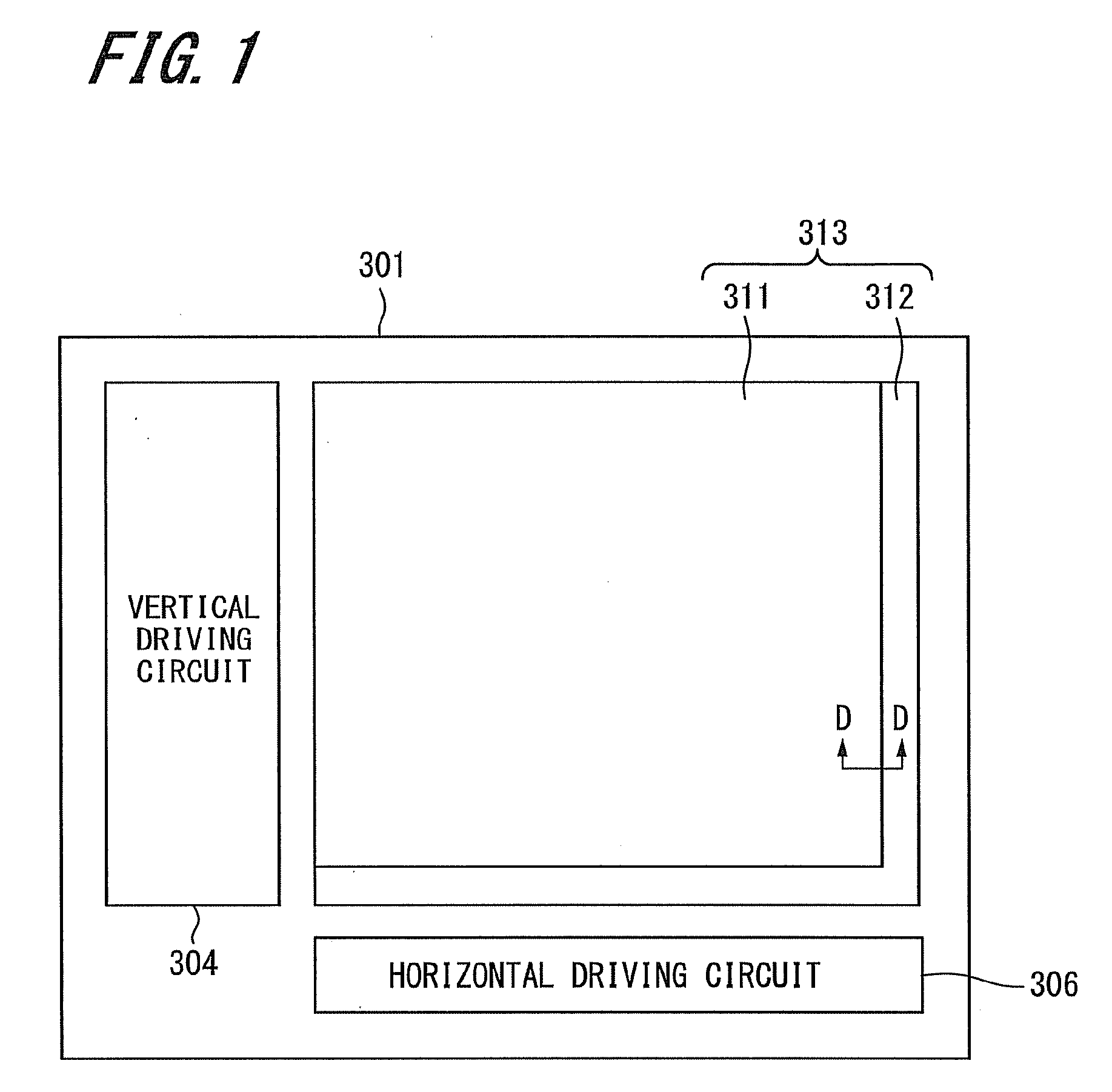
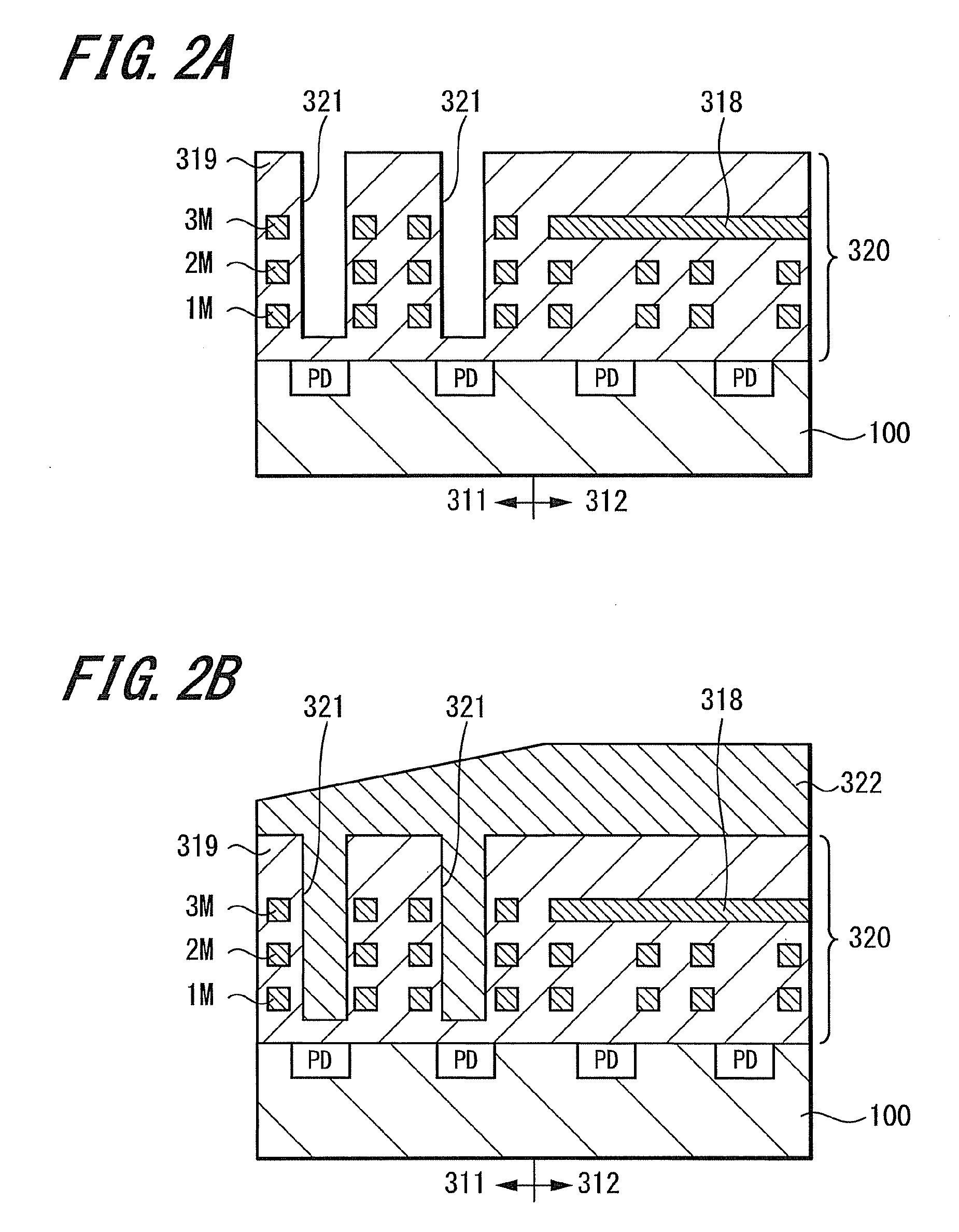
[0059]FIGS. 5A to 5C are schematic cross-sectional views illustrating a first example of a configuration of a solid-state imaging device and a method of manufacturing the same according to an embodiment of the present invention. Each of the schematic cross-sectional views of the solid-state imaging device is along the line A-A or B-B in FIG. 4, or the line extending across the effective pixel region 11 and the peripheral area 13 including the optical black region 12 and the peripheral circuit part 14. For simplified illustration, FIGS. 5A to 5C each represent only photodiodes PD (photoelectric conversion elements of the imaging pixel 2) and a plurality of wiring layers 20 thereon. In actual, the plurality of wiring layers 20 are formed above the Si substrate 100 where elements, such as pixel transistors of the imaging pixels 2 and CMOS transistors of the peripheral circuit part 14 are mounted.

[0060]The plurality of wiring layers 20 shown in FIGS. 5A to 5C includes three metal wiring...

second example

[0069]FIGS. 6A to 6C are schematic cross-sectional views illustrating a second example of a method of manufacturing a solid-state imaging device according to an embodiment of the present invention. The cross-sectional structure of the solid-state imaging device schematically illustrated in FIGS. 6A to 6C are viewed along the line A-A or B-B in FIG. 4 as in the case with the first example. In other words, it is along the line extending across an effective pixel region 11 and a peripheral area 13 including an optical black region 12 and a peripheral circuit part 14. In FIGS. 6A to 6C, the same structural elements as those in FIGS. 5A to 5C are designated by the same reference numerals and thus detailed description thereof will be hereinafter omitted.

[0070]In the present example, first, a plurality of wiring layers 20 include an uppermost metal wiring line 3M formed as a shading film 18 on a peripheral area 13 as shown in FIG. 6A. In the plurality of wiring layers 20, as shown in 6A, d...

third example

[0080]FIGS. 7A to 7C are schematic cross-sectional views illustrating a third example of a method of manufacturing a solid-state imaging device according to an embodiment of the present invention. The cross-sectional structure of the solid-state imaging device schematically illustrated in FIGS. 7A to 7C is viewed along the line A-A or B-B in FIG. 4 as in the case with the first and second examples. In other words, it is along the line extending across an effective pixel region 11 and a peripheral area 13 including an optical black region 12 and a peripheral circuit part 14. In FIGS. 7A to 7C, the same structural elements as those in FIGS. 5 and 6 are designated by the same reference numerals and thus detailed description thereof will be hereinafter omitted.

[0081]In this example, first, a plurality of wiring layers 20 include three metal wiring lines 1M, 2M, and 3M. Among them, the middle metal wiring line 2M is formed as a shading film 18 as shown in FIG. 7A. In the plurality of wir...


PUM


Abstract

A method of manufacturing a solid-state imaging device is provided. The method includes: forming an insulating layer extending over an effective pixel region where a plurality of pixels each having a photoelectric conversion element is arranged and a peripheral area adjacent to the effective pixel region; forming an opening in the insulating layer located immediately above the photoelectric conversion element on the effective pixel region; forming a dummy opening in the insulating layer on the peripheral region; and forming a buried layer on the insulating layer to fill the opening and the dummy opening formed in the insulating layer.

Description

CROSS REFERENCES TO RELATED APPLICATIONS[0001]The present invention contains subject matter related to Japanese Patent Application JP 2007-340331 filed in the Japanese Patent Office on Dec. 28, 2007, the entire contents of which being incorporated herein by reference.BACKGROUND OF THE INVENTION[0002]1. Field of the Invention[0003]The present invention relates to a solid-state imaging device with a reduction in difference in level on film thickness on the boundary between an effective pixel region and a peripheral area; a method of manufacturing such a solid-state imaging device; a camera including such a solid-state imaging device; and an electronic apparatus having such a camera.[0004]2. Description of the Related Art[0005]Heretofore, various ideas have been proposed to improve the optical characteristics of a solid-state imaging device such as a CMOS image sensor or a CCD image sensor. For improving the sensitivity of a solid-state imaging device, for example, the device is design...

Claims


Application Information

Patent Timeline
IPC IPC(8): H01L31/0352H01L21/28H01L27/14H01L27/146H04N5/335H04N5/365H04N5/369
CPCH01L27/14623H01L27/14687H01L27/14632H01L27/14603H01L27/14609
Inventor MARUYAMA, SHUNSUKE
Owner SONY CORP
Why Eureka
Try Eureka