Wired circuit board

a wired circuit board and circuit board technology, applied in the direction of printed circuit non-printed electric components association, integrated arm assembly, instruments, etc., can solve the problems of uneven suspension of discs, failure to achieve a thinner shape, and misalignment of the upper-side conductor

Active Publication Date: 2009-07-09
NITTO DENKO CORP
View PDF12 Cites 6 Cited by
  • Summary
  • Abstract
  • Description
  • Claims
  • Application Information

AI Technical Summary

Benefits of technology

[0020]When the wired circuit board is multi-layered by further forming an insulating layer and a wire, a level difference tends to be produced in the insulating layer. In this wired circuit board, since the first wire has the above-specified thickness a...

Problems solved by technology

This disadvantageously results in occurrence of unevenness in the suspension for discs.
The thicker upper-side insulating layer, however, produces a thicker suspension for discs, failing to achieve a thinner shape.
Further, in the double-decker structure, when the upper-side conductor is formed on the upper-side insulating layer having such level differe...

Method used


Image

  • Wired circuit board
  • Wired circuit board
  • Wired circuit board

Examples


example 1

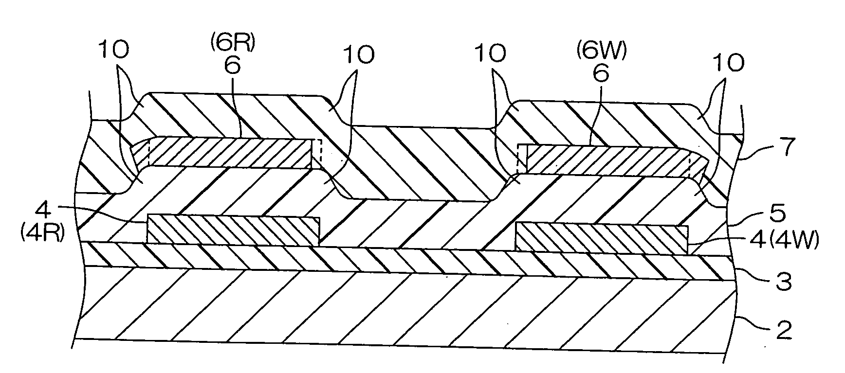
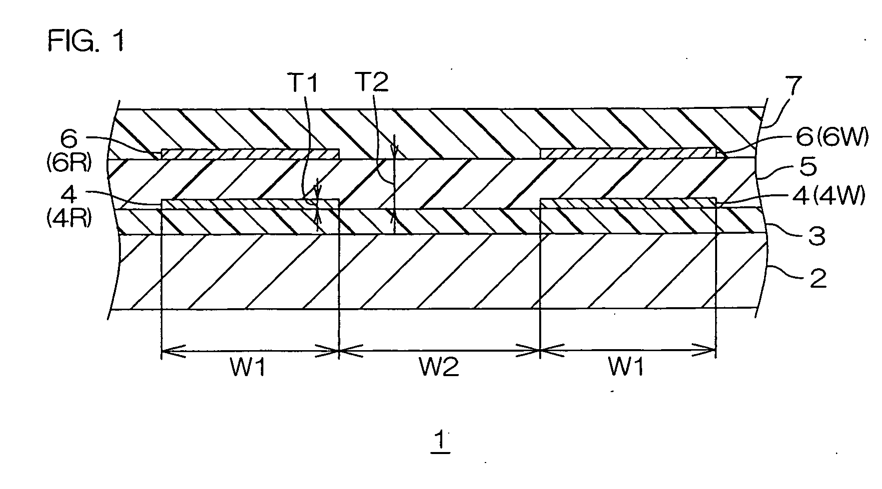
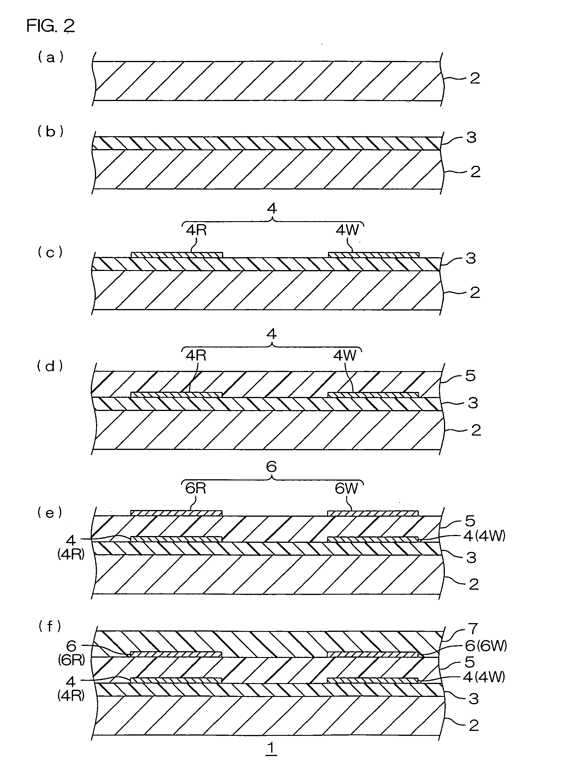
[0113]First, a metal supporting board made of a 25 μm-thick stainless steel (SUS304) foil was prepared (cf. FIG. 2(a)). A varnish of a photosensitive polyamic acid resin was then applied to the entire upper surface of the metal supporting board and then dried. Thereafter, the dried varnish was exposed to light and developed, and the obtained product was further heated to be cured, so that a 10 μm-thick insulating base layer made of polyimide was formed (cf. FIG. 2(b)).

[0114]Subsequently, first wires and first terminal portions were formed on the insulating base layer by the subtractive method (cf. FIG. 2(c)).

[0115]In the subtractive method, first, a 0.1 μm-thick first conductive layer made of copper was formed over the entire upper surface of the insulating base layer by the sputtering method (cf. FIG. 3(a)).

[0116]Then, a dry film photoresist was laminated over the entire surface of the first conductive layer. Thereafter, the laminated product was exposed to light and developed, so ...

example 2

[0130]The suspension board with circuit was obtained in the same manner as in Example 1 except that the thickness of the first wire and that of the second wire were changed to 1 μm.

example 3

[0131]The suspension board with circuit was obtained in the same manner as in Example 1 except that the spacing between each of the first wires and the width of each of the first wires were changed to the same length, i.e., 25 μm, and the spacing between each of the second wires and the width of each of the second wires were changed to the same length, i.e., 25 μm.


PUM


Abstract

A wired circuit board includes a first insulating layer; a first wire formed on the first insulating layer; a second insulating layer formed on the first insulating layer so as to cover the first wire; and a second wire formed on the second insulating layer so as to be arranged in opposed relation to the first wire in a thickness direction. The thickness of the first wire is 1 μm or less and is or less of the thickness of the second insulating layer.

Description

CROSS-REFERENCE TO RELATED APPLICATIONS[0001]This application claims the benefit of U.S. Provisional Application No. 61 / 006,602, filed Jan. 23, 2008, and claims priority from Japanese Patent Application No. 2008-000746, filed Jan. 7, 2008, the contents of which are herein incorporated by reference in their entirety.BACKGROUND OF THE INVENTION[0002]1. Field of the Invention[0003]The present invention relates to a wired circuit board. More particularly, the present invention relates to a wired circuit board such as a suspension board with circuit, a flexible wired circuit board, or a multi-layered wired circuit board.[0004]2. Description of Related Art[0005]In recent years, in order to correspond to higher wiring density, wired circuit boards such as a suspension board with circuit and a flexible wired circuit board, have been known to have, as a wiring structure, a double-decker structure such that one wire is arranged in opposed relation to another wire while an insulating layer is ...

Claims


Application Information

Patent Timeline
IPC IPC(8): H05K1/02
CPCG11B5/486H05K1/0216H05K1/0245H05K1/0248H05K2201/09736H05K2201/0352H05K2201/09236H05K2201/09672H05K1/056G11B5/484
Inventor YOKAI, TAKAHIKOOHSAWA, TETSUYAOOYABU, YASUNARI
Owner NITTO DENKO CORP
Why Eureka
Try Eureka