Electro optical device and electronic apparatus
a technology of optical devices and electronic devices, applied in the direction of instruments, discharge tubes, luminescnet screens, etc., can solve problems such as difficulty in narrowing the frame portion
- Summary
- Abstract
- Description
- Claims
- Application Information
AI Technical Summary
Benefits of technology
Problems solved by technology
Method used
Image

Examples
first embodiment
A: First Embodiment
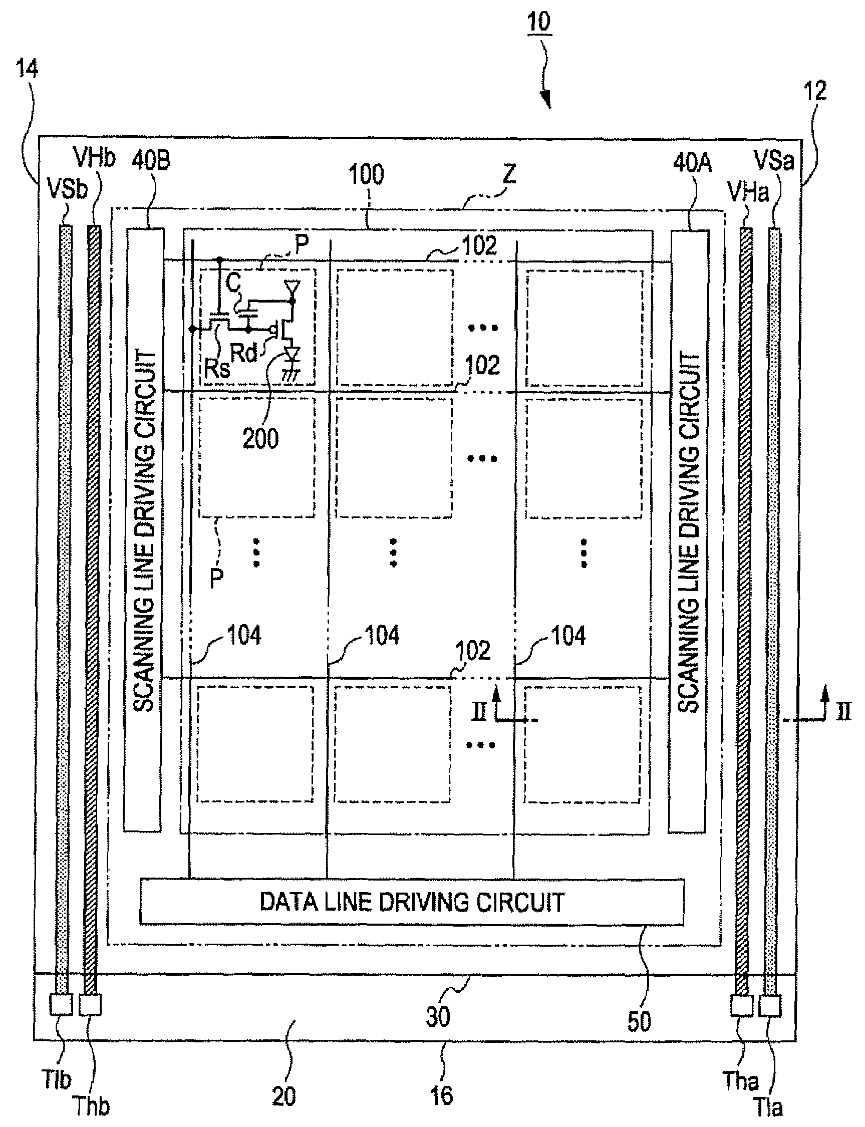
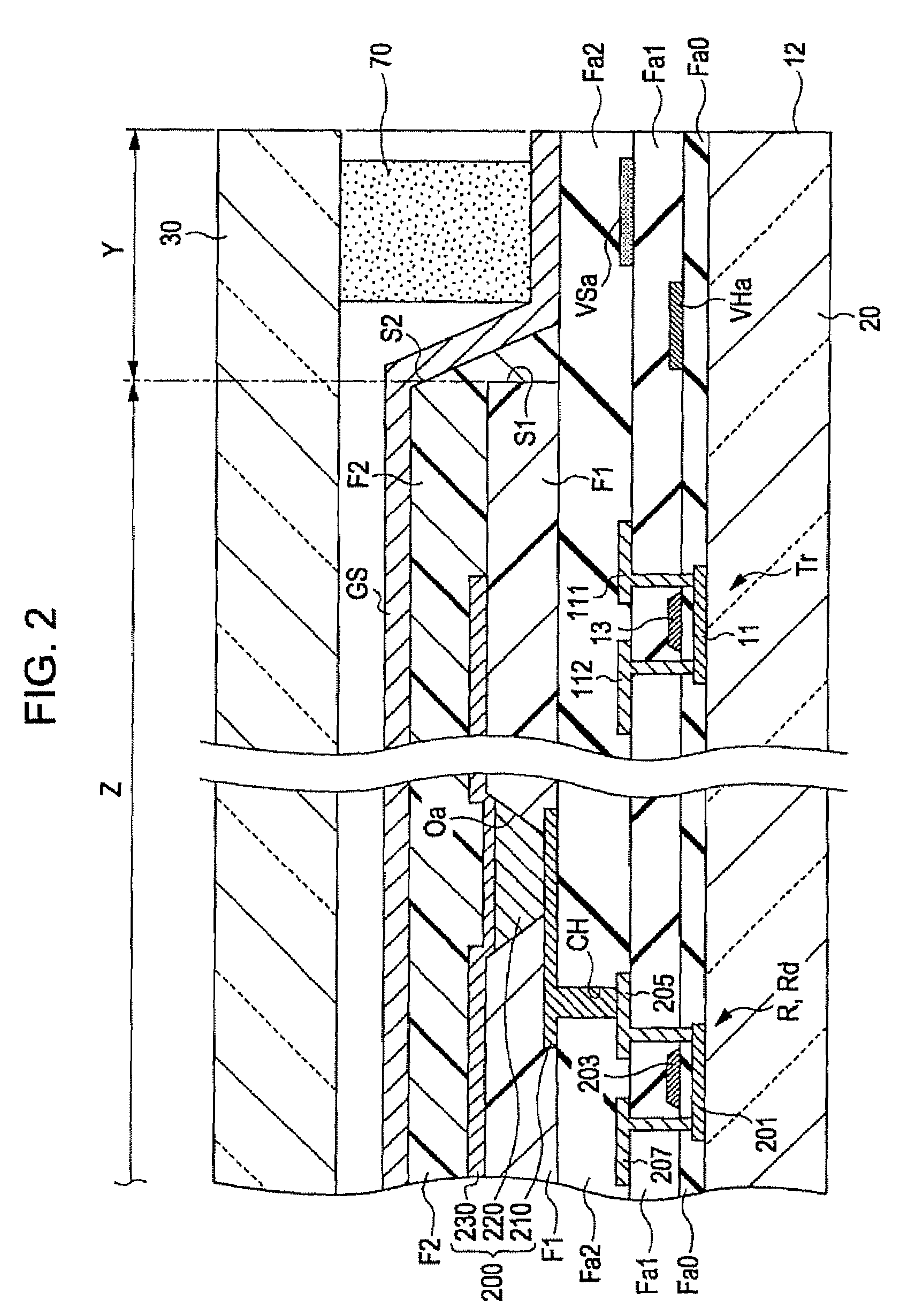
[0031]FIG. 1 is a plan view showing a structure of an electro optical device 10 according to a first embodiment of the invention. The electro optical device 10 is a device that is employed in various electronic apparatuses as means for displaying an image, and is equipped with a first substrate 20 and a second substrate 30 which are bonded to each other in an opposite state. A pixel array unit 100 in which a plurality of pixel circuits P are arranged like a plane, scanning line driving circuits 40A, 40B for driving each pixel circuit P, a data line driving circuit 50, a high potential side potential supply line VHa and a low potential side potential supply line VSa for supplying a potential to the scanning line driving circuit 40A, and a high potential side potential supply line VHb and a low potential side potential supply line VSb for supplying a potential to the scanning line driving circuit 40B are disposed on the surface of a part of the first substrate 20 op...
second embodiment
B: Second Embodiment
[0058]FIG. 5 is a cross sectional view showing the electro optical device 10 according to a second embodiment of the invention (corresponding to FIG. 3). As shown in FIG. 5, in the embodiment, the counter electrode 230 continues over the plurality of the electro optical elements 200 of the pixel circuits P and extends in the Y direction, and overlaps with at least a part of the potential supply lines via the insulating layer Fa (first insulating layer Fa1 and second insulating layer Fa2 shown in FIG. 2) covering the potential supply lines. This point is different from the structure of the first embodiment. Other structure is the same as the structure of the first embodiment, so that the description of the same structure will be omitted.
[0059]As shown in FIG. 5, the counter electrode 230 extends from the surface of the first planarizing layer F1 to the surface of the insulating layer Fa through the side surface S1. The portion of the counter electrode 230 extendin...
third embodiment
C: Third Embodiment
[0060]FIG. 6 is a plan view showing the electro optical device 10 according to a third embodiment of the invention. In the embodiment, a high potential side potential supply line VHc and a low potential side potential supply line VSc for supplying a potential to the data line driving circuit 50 are disposed on the surface of a part of the first substrate 20 opposing the second substrate 30.
[0061]The high potential side potential supply line VHc and the low potential side potential supply line VSc extend along an edge 16 of the first substrate 20 in the area outside the area Z in which the first planarizing layer F1 is provided. To be more specific, as shown in FIG. 6, the high potential side supply line VHc extends from high potential side power terminals Thc provided on the surface of the first substrate 20 along the edge 16 in the area between the data line driving circuit 50 and the edge 16 of the first substrate 20. Further as shown in FIG. 6, the low potentia...
PUM
| Property | Measurement | Unit |
|---|---|---|
| area | aaaaa | aaaaa |
| inclination angle | aaaaa | aaaaa |
| insulating | aaaaa | aaaaa |
Abstract
Description
Claims
Application Information
 - R&D Engineer
- R&D Manager
- IP Professional
- Industry Leading Data Capabilities
- Powerful AI technology
- Patent DNA Extraction
Browse by: Latest US Patents, China's latest patents, Technical Efficacy Thesaurus, Application Domain, Technology Topic.
© 2024 PatSnap. All rights reserved.Legal|Privacy policy|Modern Slavery Act Transparency Statement|Sitemap