Display substrate, preparation method thereof and display device

A technology for display substrates and display areas, which is applied in the photoplate-making process of patterned surfaces, optical mechanical equipment, transportation and packaging, etc., can solve problems such as cracks, cracks, and performance impact of display devices, and achieve the best display effect Effect

Active Publication Date: 2019-05-07
BOE TECH GRP CO LTD +1
View PDF9 Cites 17 Cited by
  • Summary
  • Abstract
  • Description
  • Claims
  • Application Information

AI Technical Summary

Problems solved by technology

The display device is prone to cracks under external forces such as collision and transportation, especially in the process of cutting to form an independent

Method used


Image

  • Display substrate, preparation method thereof and display device
  • Display substrate, preparation method thereof and display device
  • Display substrate, preparation method thereof and display device

Examples


Embodiment 1

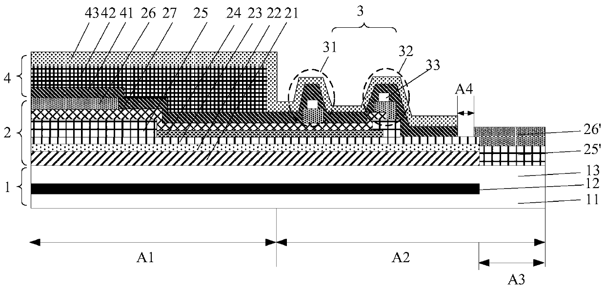
[0048] Aiming at the present situation that cracks are easily caused in the non-display area and the cracks are transmitted to the display area to affect the display performance of the display area, the present invention provides a display substrate, which has better impact resistance, so it can effectively improve the performance of the display substrate. Overall performance for a better display.

[0049] Such as figure 1 As shown, the display substrate includes a substrate 1. The display substrate is divided into a display area A1 and a non-display area A2 located on the periphery of the display area A1. The display area A1 has a plurality of pixel areas, and each pixel area is provided with a pixel structure 2. ( figure 1Only a part of the pixel structure 2 close to the non-display area A2 is shown in the figure), the pixel structure 2 includes a plurality of stacked organic film layers and inorganic film layers, and the area near the edge of the non-display area A2 is the...

Embodiment 2

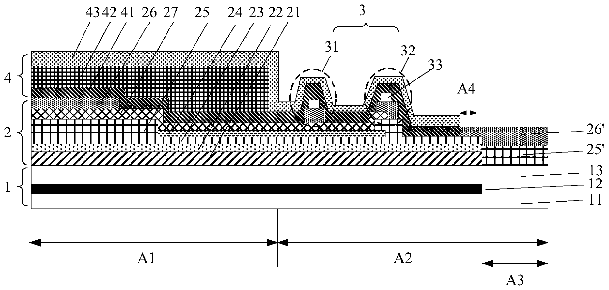
[0067] This embodiment provides a method for preparing a display substrate, which can be used to form the display substrate of Embodiment 1. As mentioned above, the display substrate includes a substrate 1, and the display substrate is divided into a display area A1 and a non-display area A2 located on the periphery of the display area A1. The display area A1 has a plurality of pixel areas, and each pixel area is provided with a pixel structure 2. The pixel structure 2 includes a plurality of stacked organic film layers and inorganic film layers.

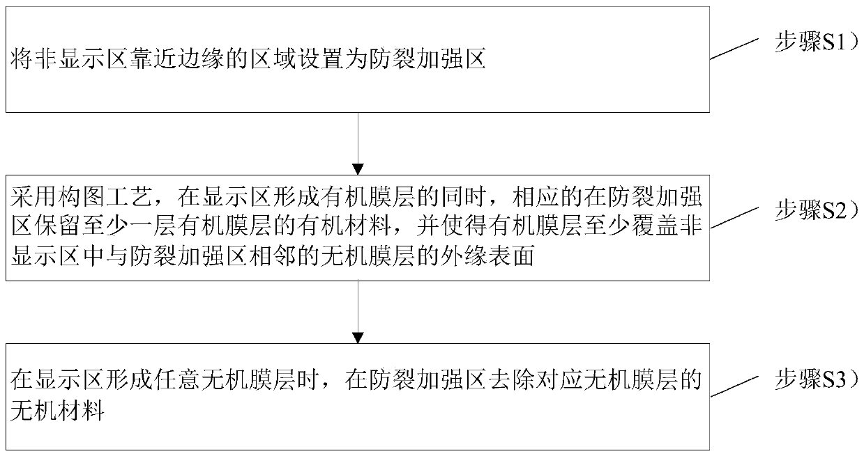
[0068] Such as image 3 As shown, the preparation method of the display substrate includes steps:

[0069] Step S1): Set the area near the edge of the non-display area A2 as the anti-crack reinforcement area A3.

[0070] In this step, the pixel structure 2 includes the control element and the light emitting device. According to the anti-crack strengthening area A3, the control element and the light emitting device are pre-planned ...

Embodiment 3

[0084] This embodiment provides a display device, which includes the display substrate in Embodiment 1.

[0085] The display device can be: desktop computer, tablet computer, notebook computer, mobile phone, PDA, GPS, vehicle display, projection display, video camera, digital camera, electronic watch, calculator, electronic instrument, instrument, liquid crystal panel, electronic paper, TV Computers, monitors, digital photo frames, navigators and other products or components with display functions can be applied to multiple fields such as public display and virtual display.

[0086] The display device can obtain better display effect.


PUM


Abstract

The invention relates to a display substrate, a preparation method thereof and a display device, and belongs to the technical field of display. The display substrate comprises a substrate, and dividedinto a display area and a non display area positioned in the periphery of the display area, the display area includes multiple pixel areas, each pixel area is provided with a pixel structure, each pixel structure comprises organic and inorganic film layers arranged in a stacked way, the region, close to the edge, of the non display area serves as an anti-cracking reinforcement region which is only provided with the organic film layer, and the organic film layer at least covers the outer surface of the inorganic film layer adjacent to the anti-cracking reinforcement region. Thus, the inorganicfilm layer is fundamentally prevented from a crack caused by an outside force, crack transfer is eliminated, and further, the framework is narrowed, the anti-impact performance of the display substrate is improved, the cutting energy is reduced, the cutting yield rate is improved, and the cutting effect is improved.

Description

technical field [0001] The invention belongs to the field of display technology, and in particular relates to a display substrate, a preparation method of the display substrate, and a display device. Background technique [0002] In the new generation of display devices, display modes such as organic light emitting devices (Organic Light Emitting Diode, referred to as OLED) and quantum dot light emitting devices (Quantum Dots Light Emitting Diode, referred to as QLED) have the advantages of bright colors, low power consumption, thin and flexible It has become a current research hotspot. Organic light-emitting devices and quantum dot light-emitting devices are easily corroded by water and oxygen and become invalid. Generally, thin film encapsulation (Thin Film Encapsulation, TFE) is used to isolate the light-emitting materials from water and oxygen. [0003] In the current production line, a plurality of display device areas are laid out on the display substrate (Panel), a p...

Claims


Application Information

Patent Timeline
IPC IPC(8): H01L51/52H01L51/56H01L27/32
CPCH10K59/122H10K59/124H10K50/80H10K50/844H10K2102/351H10K71/851G03F7/0007Y10T428/24579Y10T428/24612H10K50/841H10K71/00
Inventor 宋丽蒋志亮毛明
Owner BOE TECH GRP CO LTD
Why Eureka
Try Eureka