Methodology for improving device performance prediction from effects of active area corner rounding

a technology of active area corner rounding and device performance prediction, which is applied in the direction of electric/magnetic computing, analogue processes for specific applications, instruments, etc., can solve problems such as performance negatively affecting performan

Inactive Publication Date: 2009-07-09
IBM CORP
View PDF10 Cites 5 Cited by
  • Summary
  • Abstract
  • Description
  • Claims
  • Application Information

AI Technical Summary

Benefits of technology

[0018]updating transistor model parameter values in a transistor compact model for the transistor device to include deltaW adder values to be added to a built-in deltaW value, wherein a netlist used in a si...

Problems solved by technology

In essence, lithographic constraints are conventionally determined by the generally limited capability of a lithographic process to successfully print line features at specified positions within tolerance...

Method used


Image

  • Methodology for improving device performance prediction from effects of active area corner rounding
  • Methodology for improving device performance prediction from effects of active area corner rounding
  • Methodology for improving device performance prediction from effects of active area corner rounding

Examples


Embodiment Construction

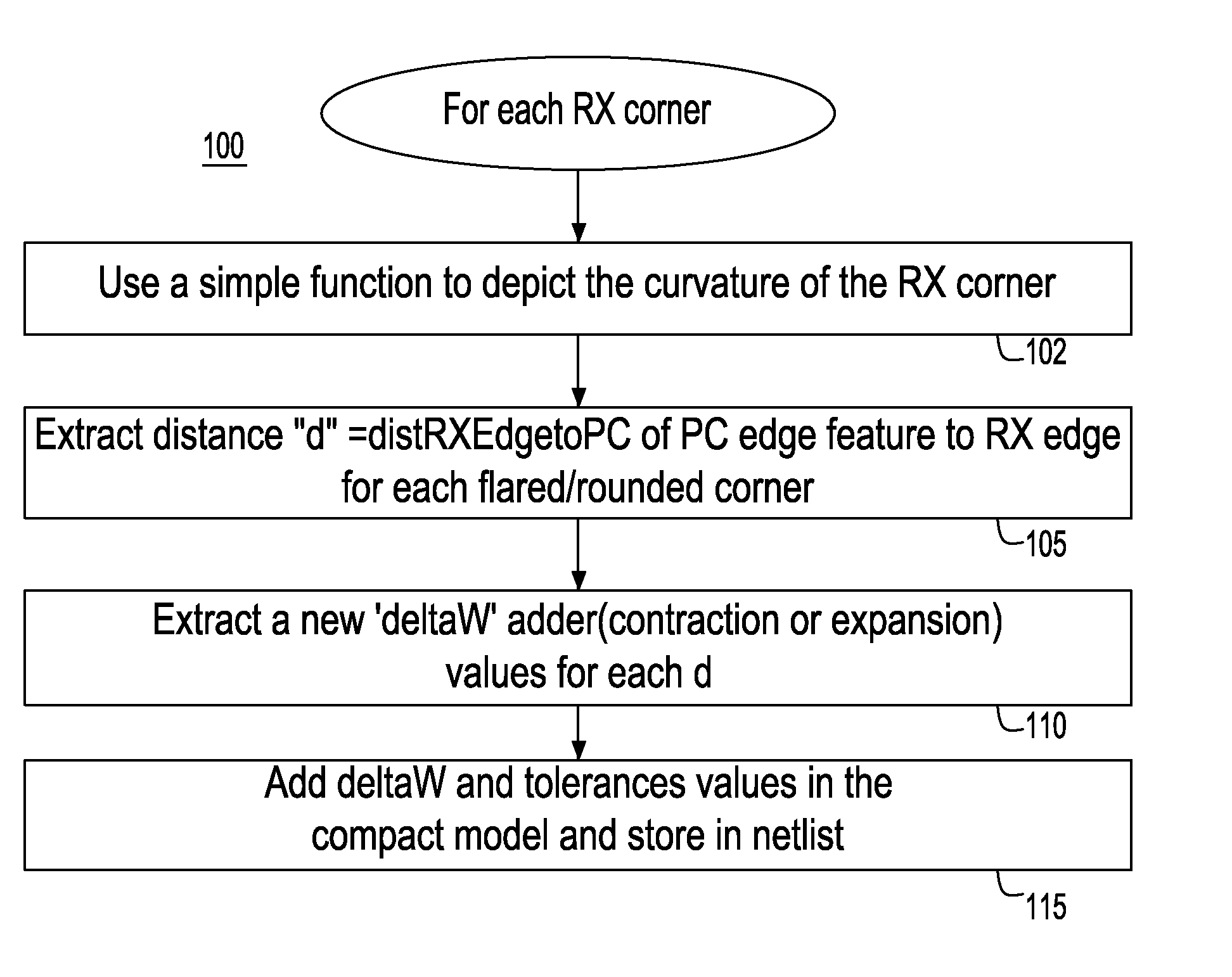
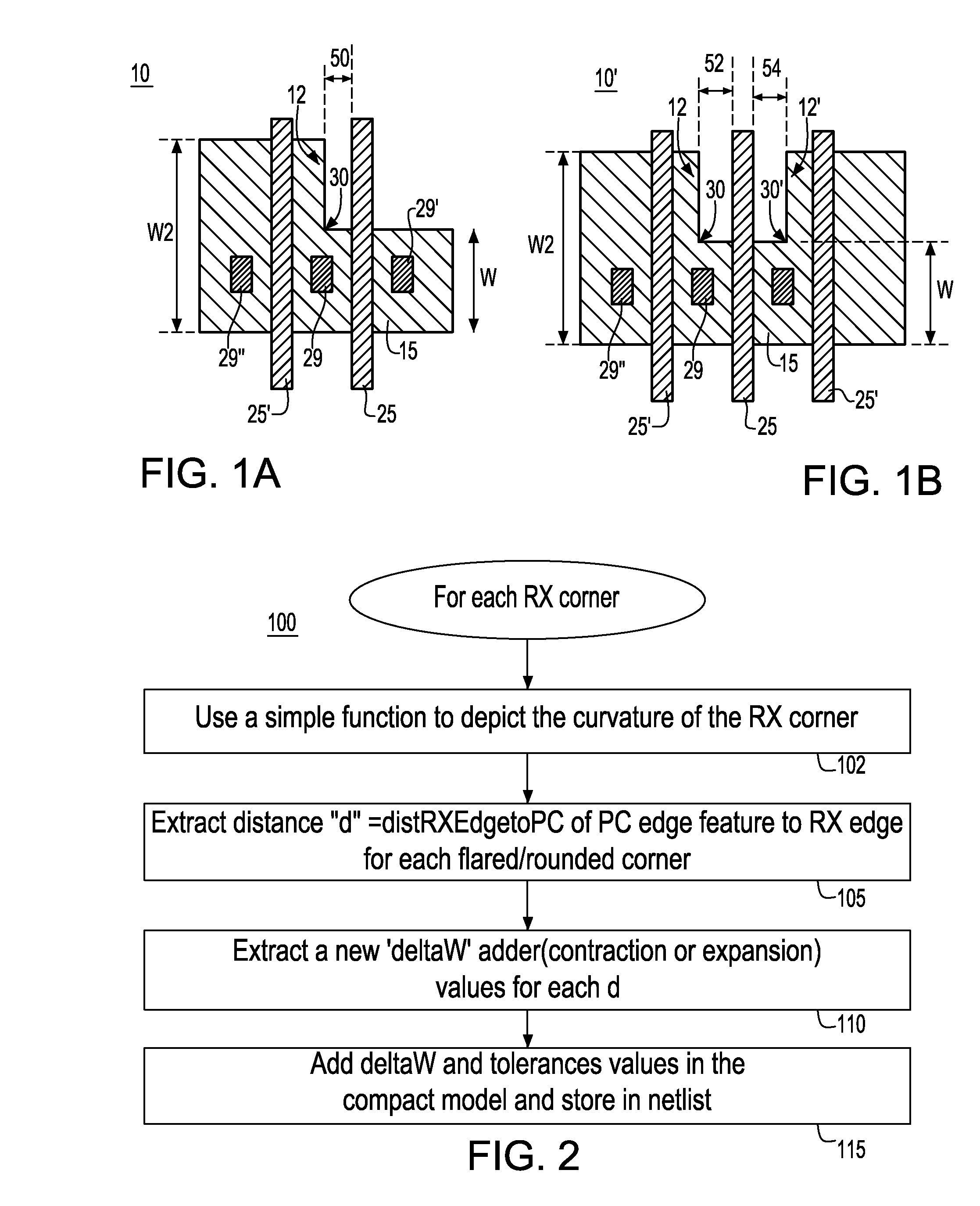
[0025]FIG. 2 depicts a methodology flow 100 according to one embodiment of the invention. It is understood that the method depicted will apply for each individual RX corner being modeled. In the method depicted, an analytical model is presented that includes a first step 102 that implements a simple function to depict the curvature of the flared RX corner region as shown in FIGS. 1A, 1B. In step 102, this model may be obtained by performing an RX lithographic contours analysis and from which an analytical model formulation with input choices based on the lithographic contours analysis is developed. In one embodiment, a contours analysis model is a geometric function, e.g., a circle, to determine the corner rounding description. In alternative embodiments, other geometric functions or combinations of functions (parabolas, triangles, etc.) may be used for the model; however, it has been determined that a circle function sufficiently fits the RX rounding effects, for example.

[0026]Furt...


PUM


Abstract

A system and method for modeling a semiconductor transistor device structure having a conductive line feature of a designed length connected to a gate of a transistor device in a circuit to be modeled, the transistor including an active device (RX) area over which the gate is formed and over which the conductive line feature extends. The method includes providing an analytical model representation including a function for modeling a lithographic flare effect impacting the active device area width; and, from the modeling function, relating an effective change in active device area width (deltaW adder) as a function of a distance from a defined edge of the RX area. Then, transistor model parameter values in a transistor compact model for the device are updated to include deltaW adder values to be added to a built-in deltaW value. A netlist used in a simulation includes the deltaW adder values to more accurately describe the characteristics of the transistor device being modeled including modeling of lithographic corner rounding effect on transistor device parametrics.

Description

BACKGROUND OF THE INVENTION[0001]1. Field of the Invention[0002]The present invention relates to a novel method and system for optimizing integrated circuit layouts, generally, and particularly, a system and method for modeling performance of a semiconductor device structure for achieving modified ground rules for lithographic feature distances that optimize semiconductor device performance.[0003]2. Description of the Prior Art[0004]Lithographic constraints are important factors in determining the efficiency of a circuit layout. In essence, lithographic constraints are conventionally determined by the generally limited capability of a lithographic process to successfully print line features at specified positions within tolerances. A lithographic process involves using a lithographic exposure tool to illuminate a lithographic mask from a range of directions, and focusing a projected image of the mask onto a photosensitive film that coats a partially fabricated integrated circuit on ...

Claims


Application Information

Patent Timeline
IPC IPC(8): G06F17/50
CPCG06F17/5036G06F30/367
Inventor CHIDAMBARRAO, DURESETIDAVIDSON, GERALD M.HYDE, PAUL A.MCCULLEN, JUDITH H.NARASIMHA, SHREESH
Owner IBM CORP
Why Eureka
Try Eureka